This thread has been locked.

If you have a related question, please click the "Ask a related question" button in the top right corner. The newly created question will be automatically linked to this question.

LM3409HV: Unexpected second toff

Part Number: LM3409HV
Other Parts Discussed in Thread: LM3409

Hello,

we are experimenting unexpected second toff using LM3409HV.
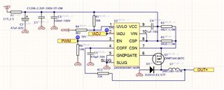
The schematic is reported below, please note that R3 is not fitted, then Rsns=0.3ohm.
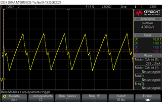
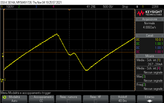
The IADJ pin is controlled to  have an avg led current of 350mA. The toff time is around 500ns as expected and the inductor ripple current (around 200mA) is higher than 24mV/Rsns limit of 80mA.

In the scope image the second toff problem reported in the chapter 8.3.4 of the datasheet is present. 
Could you please help me to understand why there's a second toff? 

Thank you,
Daniele

  • Hello Daniele,

    I would look at section 9.1.8.  This doesn't look like the error amplifier offset this looks like the LM3409 is tripping peak current sense a second time, this is common with larger MOSFETs, high Vth MOSFETs, non-schottky freewheel diode or too large a gate resistor.  It doesn't seem like the components used would cause this however 350 mA is low for the MOSFET chosen and Qgate is close to 30 nC.  You may be able to see this looking across the current sense resistors to see if it is hitting peak current trip after the leading edge blanking time (115 ns, 211 ns maximum).  The second on-time looks to be about minimum on-time (around 150 ns on the scope picture above).

    "When using a PFET with Qg > 30nC, the bypass capacitor (CF) should not be connected to the VIN pin. This will
    ensure that peak current detection through RSNS is not affected by the charging of the PFET input capacitance
    during switching, which can cause false triggering of the peak detection comparator. Instead, CF should be
    connected from the VCC pin to the CSN pin which will cause a small DC offset in VCST and ultimately ILED,
    however it avoids the problematic false triggering."

    Best Regards,

  • Hello,

    thank you for your prompt support.
    Could you please help me to clarify which is the "leading edge blanking time"?

  • Hello Daniele,

    Leading edge blanking time, minimum on-time, is to prevent the peak current trip from happening due to the added current during the MOSFET turn-on.  When the MOSFET is turning on there is added current from the MOSFET switching on going through the current sense resistor.

    Things that can cause the LM3409 to prematurely trip the peak current threshold are:

    Large MOSFET with high Qgate

    MOSFET with high VGS threshold

    A freewheel diode that has a hard recovery

    A gate resistor that delays the MOSFET turn on past the leading edge blanking time

    Best Regards,