This thread has been locked.

If you have a related question, please click the "Ask a related question" button in the top right corner. The newly created question will be automatically linked to this question.

UCC28633: No load, low-power sleep mode

Part Number: UCC28633
Other Parts Discussed in Thread: UCC28630

Hello,

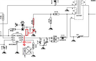
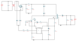
I've made a flyback schematic with the UCC28633. 
110VAC to 230VAC input, 40VDC 2A output. 

With no load/light load i have the following behaviour.
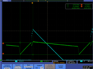
VDD goes up with HV current source.
Line UV check pulses are send.
And switcher starts with normal PWM at 30kHz.
VDD settles around 12V.
Switcher regulates till Vout is around 40V.
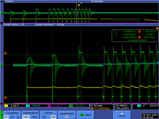
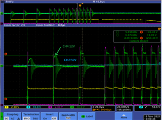
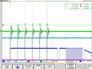
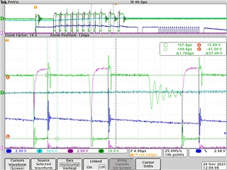
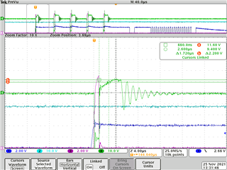
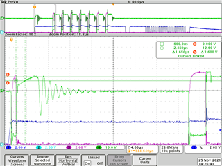
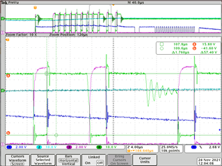
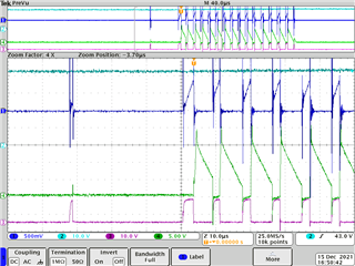
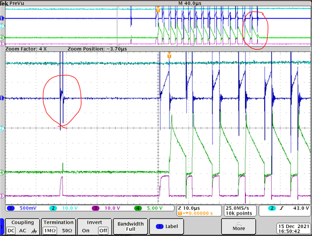
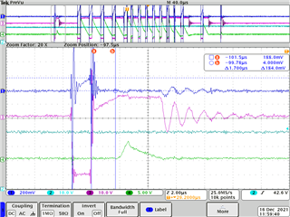
Due to light load, the switcher goes to around 15kHz and goes in sleep mode? 
The SD pin goes low for a short while (20us). 
The SD pin goes high again for the next switch pulse and remains high for about 45us after the pulse.
Due to the lowering switch frequency the duration of SD low increases. 
Last measured time between 2 pulses is 365us or 2,7kHz.

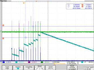
The device goes into a sleep mode?

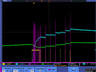
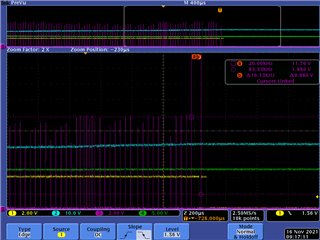
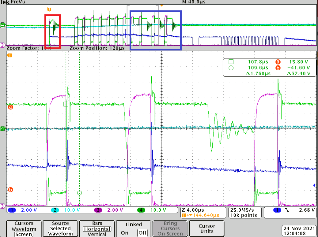
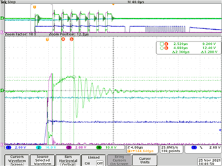
After about 5ms (200Hz) I see the device restart it pulses.
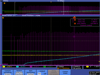
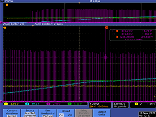
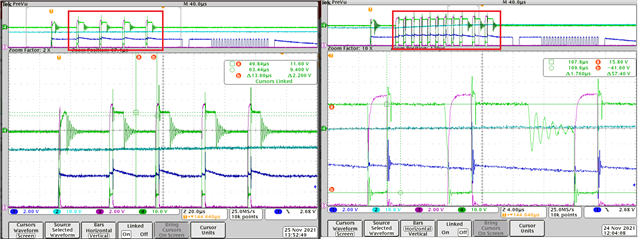
It sends 1 shot pulse (pulse width of 600ns)
It waits for 32us 
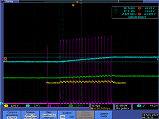
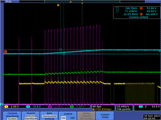
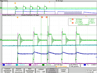
then sends 17 pulses where Vcs goes to 880mV (pulse width is around 2us)
The frequency of those 17 pulses is 122 kHz
The sequence ends with another short pulse 250ns.

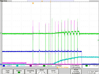
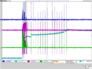
Each time such a sequence happens the output voltage increases.
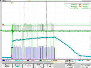
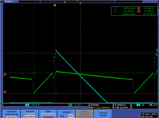
This lasts until the switcher detects that the Vout is to high and goes in Fault mode with auto restart.

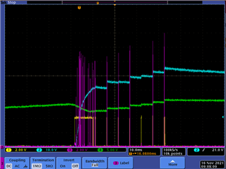
If I increase the output with several whats, the switcher continues to operate. 

Can you point me in the derection to optimize my schematic so it works with low loads as well? 

  • Hi, Wouter:

    Thanks for reaching out us. 

    About your questions, please check the figure shows below, or you could find it on page 48 in datasheet. 

    If the switching frequency of UCC28633 is around 200Hz ~ 30KHz, and VCS is around 170mV, IC operates in sleep mode. It would turn off several block inside IC to save more power. Thus, it is correct that you mentioned SD would be deceased during gate signal off. 

    When fs is 120kHz, and VCS is 0.8V, the IC is in peak load operation. 

    I would like to clarify the phenomenon you meet.

    * IC start-up and fs is 30kHz, and operates as 15kHz after Vo is 40V.  fs keeps decreasing to 200Hz after 5ms,

    (So the fs is 30KHz --> 15kHz --> 2.7kHz --> 200Hz, is it correct?)

      *Once fs is 200Hz, the fs increases to 120kHz in a very short time(32uS), and Vo is raised by this high frequency, and trigger VDD OVP fault.  ( If it triggered VS OVP, the protection mode would be latched off) 

    Based on my understanding as below, would you please check if there is significant drop of VDD and Vout when fs is 200Hz?

    If the Vo is flat or does not change a lot. You may check if there is any noise impact the Vsense signal because the there is a wake-up function build in UCC28633's Vsense pin. The UCC28633 can respond to fast transient wake signal coupled to the VSENSE pin. If the wake signal exceeds an internal pin threshold VSENSE(wake) while the controller is in sleep mode. 

    Please measure VAUX waveform instead of Vsense waveform to avoid noise goes through Vsense during the measurement. Also, VAUX can provide the output voltage information and may provide some clues when fs switches to 120kHz from 200Hz. 

    If it is no concern, please share the waveform you measure by using "insert" function to upload them in E2E. It is helpful to know more clear the issue you meet. 

    Thank you very much. 

    Regards, 

    Wesley  

  • Hello Wesley,

    Thank you for your reply.

    To answer on your question, Vout and VDD are going low and below reset level.
    This sequence repeats every 1,3s.


    Ch2: Vout    Ch4: VDD


    I analysed one iteration. 

    First switching cycle the Vou goes to 40V.
    Device goes in sleep mode. Then every 5ms it sends some pulses that increase the Vou until 55V and the device goes in OVP.


    Close up from start: First the 3 UV check pulses at 15kHz
    Image 1
    Ch1: Vsd    Ch2: Vout    Ch3: Vdriver at FET    Ch4: VDD


    Than several 30kHz pulses for about 1ms, Vout is inclining from 0V to 15V.
    Than freq goes up to around 60kHz (lasts 600us), untill Vout reaches 20V.

    Ch1: Vsd    Ch2: Vout    Ch3: Vdriver at FET    Ch4: VDD

    Keeps on regulating between 15/30/60 kHz untill Vout is 40V.
    The regulation is not in declining order.
    But some times it goes up, sometimes down in frequency.

    Ch1: Vsd    Ch2: Vout    Ch3: Vdriver at FET    Ch4: VDD

    When Vout is reached. It stops regulating and Vsd goes to a low state.
    Device is entering powendown mode?

    After around 5ms it starts switching at 125kHz

    It does this several times untill Vout reaches OVP

    First the frequency is 30kHz for 2 pulses (number can vary) but then it goes to 125kHz.
    Vout goes from 50V to 54V and OVP starts working. 

    I've also measured Vaux at the time of the last pulses before OVP trades in.

    My schematic

    If you need more info or measurements, please ask.

    Thank you for your help.
    With kind regards,

    Wouter

  • Hi, Wouter:

    Thanks for your sharing. I thought this phenomenon is caused by improper VS signal in this time. 

    In the beginning, please move R178 and C150 to the location as below.  (the refer design is as UCC28630 EVM )

    According to the waveform you shared, the VAUX is 12V~13V around as Vout(CH2) is 50V. VS is around 6.78V~7.34V

    The VS should be equal to 7.5V to regulate the output voltage. Vaux sent a incorrect signal to VS pin to let UCC28633 increases DRV frequency. 

    Would you please check the Naux/Nsec, R175 and R176 value are proper. I used the equations on page 65 in datasheet and got a briefly calculation results that R175 would be 18kohm and R176 would be 47.44kohm.  Since I have no turns information of Naux and Nsec, I assumed their value based on the waveform. So need your help to check VS setting.  

    Regards,

    Wesley

  • Hello Wesley,

    I tried your suggestions. But the problem remains.
    It takes longer to reach the OVP. Also Vout goes to around 40V untill OVP starts.


    Ch1: Vsd    Ch2: Vout    Ch3: Vdriver at FET    Ch4: Vaux


    Ch1: Vsd    Ch2: Vout    Ch3: Vdriver at FET    Ch4: Vaux

    I count 20 pulses on the Vsd channel, so the reason is OVP.
     
    The transformator is custom build and I have these specs:
    Turn ratio Sec/Pri = 0,364
    Turn ratio Pri/Aux = 0,121
    (Calculated Sec/Aux = 3)

    Lpri = 168uH
    Lpri leakage = 1uH


  • Hi, Wouter:

    I used the sepc. that you share and get the results as below. Would you please try this parameters first?

    R175 = 20kohm

    R176 = 50kohm

    R360 = 100mohm

    Add a Rdummy check if the phenomenon improves, based on the calculation, you may use Rdummy and starts from  15kohm . 

    Regards, 

    Wesley 

  • Hi Wesley,

    Added the values above but need to use 51k for R176.
    No improvement. It got worse.


    Ch1: Vsd    Ch2: Vout    Ch3: Vdriver at FET    Ch4: Vaux

    Zoomed in on the very first switching sequence

    Ch1: Vsd    Ch2: Vout    Ch3: Vdriver at FET    Ch4: Vaux

    With kind regards,
    Wouter

  • I needed to add 3W to let it start with continuous regulation. but not the good Vout 17V (3W at 17V)

    Increasing the load to 7W, I get propper regulation with no audible noise . But also with 31V output voltage.

    Are you sure about the 20 and 50k for the resistor?

    Thank you for your assistance.
    With kind regards,

    Wouter

  • Hi, Wouter:
    The 20k and 50k comes from the equations which shows in datasheet. It should be correct.  One possible is the voltage sensing point is not flat enough or not as same value as we expected to make this error happen. As you can see the voltage sensing delay time is 1.7us after DRV off. If there is still a ringing on Vs after DRV off for 1.7us. It could impact the output voltage regulation. Would you mind to check it because It is hard to me read the accurate value based on the previous waveform. The sense error of Vs pin could be the root caused to make this phenomenon that you meet 

    It's a limitation of PSR topology since it only can get output information by auxiliary wilding, which is impact by lots of factors...

    So you may put the R175 and R176 back and only add a dummy load to see if the abnormal phenomenon improved.

    Regards,

    Wesley

  • Hello Wesley,

    Srry for my late reply. Some other work got priority.

    I have a scope image of the last sequence before the regulator goes in OVP.

    Ch1: Vsd    Ch2: Vout    Ch3: Vdriver at FET    Ch4: Vaux

    The vertical cursor is standing 1,7us after driving the FET.
    We have a steady Vaux of 15,8V at Vout of 51V.
    Measured Sec/Aux = 3,22 or Aux/Sec = 0,309

    I also measured Vin DC = 340V. When FET is on, Vaux is -41.60V
    So measured Aux/Pri =  0,122 (comparable with the info from the manufacturer).

    With kind regards,

    Wouter

  • Hi, Wouter:

    Would you mind the check the Vaux sample point in red area? I would like to check the Vout/VDD/VAUX in this moment. It is because after the first pules, the fs increase fast. The fs decreases in blue seems correct because IC senses the the output voltage is high. 

    Did you ever try to change the value of C150? Is it getting better or worse when you increase it?

  • Hello Wesley,


    Ch1: Vsd    Ch2: Vout    Ch3: Vdriver at FET    Ch4: Vaux

    1,7us after the FET is driven, it is 9,4V. 
    2,7us after the FET is driven, Vaux is 11,60V.


    For the 4 other sequences Vaux starts at 11,60V.

    Ch1: Vsd    Ch2: Vout    Ch3: Vdriver at FET    Ch4: Vaux

    Measuring the VDD gives a 14V with some smal spikes while switching.
    So that doesn't pull the Vaux low.

    If I understand you correctly, the switcher measures the Vaux 1,7us after driving the FET.
    It then measures a value that is to low (9,4V). Will increasing the C150 not making it worse?

    I've change the C150 to 22pF. And focussed on the first pulse.

    Ch1: Vsd    Ch2: Vout    Ch3: Vdriver at FET    Ch4: Vaux

    1,7us after the FET is driven, it is 9V. 
    2us after the FET is driven (max value), Vaux is 12,60V.
    Vout is 43V

    I've change the C150 to 6,8pF. And focussed on the first pulse.

    Ch1: Vsd    Ch2: Vout    Ch3: Vdriver at FET    Ch4: Vaux

    1,7us after the FET is driven, it is 9,2V. 
    2,4us after the FET is driven (max value), Vaux is 12,60V.
    Vout is 43V


    With kind regards,
    Wouter

  • Hi, Wouter

    Yes, to increase C150 should make this condition getting worse.

    Because I am getting confused about the waveform you shared, I would like to check if this is caused by noise. 

    In the beginning, the waveform you shared as below.

    The waveform is correct. The max VDD(Green) is around 17V, which could trigger VDDOVP to shut down the IC. 

    And the 2nd one shows the frequency is 200Hz (5ms), which is also correct because IC operates in sleep mode. Since this is PSR, it is needed to force switching to sense output voltage. So the output is getting higher because of the force switching every 200Hz. 

    The 3rd waveform shows the fs in the burst package. As you can see the Vout(CH2) is around 40V, which is the target output. However, the fs goes to 125kHz. This frequency is too high to regulate output. So I thought there might be something wrong about VS sensing. 

    The waveform also shows the similar symptom. The fs is high even the Vout is out of regulation. 

    So I doubt VS could be impact by some noise. If there is a noise to make VS sensing error, it would be helpful if C150 increased. 

    However, the latest waveform you shared (as the below left) seems IC operates in normal burst. It confused me because it shows the normal operation of PSR burst mode. Is the test condition different? 

    Regards,

    Wesley

  • Hello Wesley, 
    It is possible I used a different load setting on my electrical load.
    But still low enough to trip the OVP. 

    I've changed the divider when you told me to make it 20k en 50k (20k and 51k is used).

    Then I changed the C150. 
    First measurement was C150 = 10pF.
    I then changed it to 22pF en 6,8pF.

    No other hardware is changed.

    The switcher measures 1,7us at the first pulse.
    Is the signal OK? because it doesn't has a steady level like the next pulses.
    What could be the reason of the increasing value? The Vout is steady.
    Do the switcher measures every time after driving the FET? Or just the first time?
    And than again after a particular time?

    With kind regards,

  • Hi, Wouter, 

    I assume you get this issue resolved.

    If not, let us know what else you have tried.

    Best regards,

    Don

  • Hello Don,

    No the issue is not resolved.
    I still haven't a stready supply with low load. 
    The switcher goes in OVP.
    I was waiting for a reply on: 

    "The switcher measures 1,7us at the first pulse.
    Is the signal OK? because it doesn't has a steady level like the next pulses.
    What could be the reason of the increasing value? The Vout is steady.
    Do the switcher measures every time after driving the FET? Or just the first time?
    And than again after a particular time?"

    Maybe this can lead to a solution.

    With kind regards,

  • Hi, Wouter:

    Sorry for my late.

    The first signal is not okay since it is not stable. So IC actually read the wrong value to generate next DRV signal. but the updated time after IC sampled the Vaux value is slow.  It is a reason of the increasing value. 

    To verify this assumption, would you please check if the 1st DRV width is closed to ton,min (600ns as typ).?  Please increase C149 to extend the 1st DRV width. It is helpful to let IC read the correct value. 

    Regards,

    Wesley

  • Hello Wesley,
    Also srry for my late reply. The measured first pulsewidth is 810ns. I didn't had the time to change the capacitor.
    I'll do it tomorrow. 
    I've also noticed that the sense resistor R360 = 100mOhm. I changed the value some test ago. 

    *Update: Changed the value to 150pF
    The first pulse is increased to 1,320us

     Then i've changed the value to 68pF
    and the pulse went back to 960ns.

    On a new board with no changes on the schematic:
    Sometimes it runs for a short while with working regulation.
    Then it goes into OVP and tries to start. So on...

    On this board I've measured the current in the secondary side.
    For the first pulse of 860ns, there is almost no flyback current.
    Measuring the voltage over R360 confirms this.

    Ch1: V_R360    Ch2: Vout    Ch3: Vdriver at FET    Ch4: I secondary (1V/1A)

    So the first pulse of 860ns doesn't last long enough to generate a primary current?
    Because there is no energy in the transformer, no secondary current is generated.
    Because there is no secondary current, no Vout measurement can be done.

    Is this a problem? That the Vout can't be measured due to the first pulse.
    Is this the reason that the regulation is not working? 
    Are this aditional checks in this sequence of the Vout or is it only with the first pulse?

    With kind regards,

    Wouter

  • Hi, Wouter:

    Yes, I thought it would be one of the reason. So let us solve this issue first. 

    The waveform of R360 seems very noisy. There is a huge overshoot and undershoot when gate on/off on the waveform. So it is hard to check if the gate turns off because of real signal or noise. 

    When IC goes to sleep mode, the Vcs(limit) would be 170mV around to regulate output. So please try to increase Lpri (maybe 200uH~230uH) or decrease R360 to support more energy to secondary side after you checked the waveform on CS pin (pin3 or C149). 

    About your questions, yes, IC would check the Vout not only with 1st pulse, however, the response is slow. 

    (You can see it operates in CCM first and goes to DCM. It shows IC is doing the regulation but the speed is not fast)

    As you can see the gate shrink and stops after several pulse but it eventually caused Vout increase because of the slow response. 


    Regards, 

    Wesley

  • Hi Wesley,

    With the last board and 150mOhm for R360, I had a situation where it was regulating the board for short periods of time.

    I've changed the value of R360 to 75mOhm.
    The Vaux is better at the time of switch off, but not perfect.

    Ch1: V_R360    Ch2: Vout    Ch3: Vaux    Ch4: I secondary (1V/1A)

    Vaux comes up slowly, due to the low current flowing in the transformator.
    1,7us after the driver is switched off, Vaux is at the Vout level.
    So I believe a correct measurement is done.

    But now it almost immediately runs in OVP.

    Ch1: V_R360    Ch2: Vout    Ch3: Vaux    Ch4: I secondary (1V/1A)

    But I'm starting to figure it out. 
    It starts up and does his regulation until the Vout is high enough.
    Then is goes in to a mode where it reduces his regulation.
    Every 5,28ms is check's its Vout to see if extra regulation is necessary.
    By doing this check, is also drives the Vout to a slightly higher level.
    These check's continue untill Vout hits OVP.

    How can i solve this,
    so that the power going into the output is not higher then the load on the output?
    Can I increase the speed of the switcher? With less pulses, less power goes into the output.
    Increase R360? But then we have not enough power into the output so no decent measurement can
    be performed on the Vaux...

    With kind regards,
    Wouter

  • Hi, Wouter: 

    It starts up and does his regulation until the Vout is high enough.
    Then is goes in to a mode where it reduces his regulation.
    Every 5,28ms is check's its Vout to see if extra regulation is necessary.
    By doing this check, is also drives the Vout to a slightly higher level.

    Yes, IC checks Vout through auxiliary winding because it is PSR. So the concepts are 

    1st, it is needed to make sure the Vaux voltage reflects output voltage correctly. 

    2nd, a dummy load is needed in output side to consume the extra energy by the Vout checking behavior. 

    To decrease Rcs(R360) is to increase the energy of 1st pulse to get proper Vaux, but it also delivery more energy to output side in each pules. 

    Would you mind to enter the parameter that you used in the calculation file ? (UCC28633 calculator

    And then share it to me? When I inputs the parameters that you shared, it shows the Lp should be higher than 168uH.  I am not sure if my input is still aligned with your value now. You may use it to check the transformer necessary inductance and it is helpful to make us in the same page.

    Thanks. 

    Regards,

    Wesley 

  • Hello Wesley,

    I didn't use the calculator. Ive used the Ti web bench power designer.
    With input parameters: 

    Input: 
    AC 85 V - 265 V at 60.0 Hz
    Output: 
    Isolated 40 V at 2.5 A
    It generated this schematic:
     

    We made a custom transformer with the specs:


    Last time I've checked, was the minimun load to add for proper regulation, 5W extra.
    The problem is, that this board needs to work for test purpose before some loads are added.
    So it needs to work with light loads ( and heavy loads (50- 60 W)
    With kind regards,
  • Hi, Wouter:

    I still suggest you to key in your existing parameters into the calculator since it has lots of configuration of UCC28630. It's tool to check each setting. 

    It's more detail than Web bench designer, and there are some difference between the web bench designer and your schematic. i.e. R175=30kohm, R178=39kohm; R1= 28kohm and R2=26.1kohm. I did not find your RBLD value, either. 

    So could you please fill in your parameters into calculator and share it to me?

    We could discuss with in email if you thought some of the information are suitable to show in the forum.

    Thanks. 

    Regards,

    Wesley

  • Hello Wesley,

    I've filled in the calculator with the parameters I know.
    But I didn't have the information of the core section.
    At the bottom I have the notification that my Rcs/Lpri is not OK.
    I need to increase Lpri or decrease Rcs. 

    I'm not able to increase the Lpri. And the calculator is not able to adjust the Rcs.

    What do you mean by RBLD? Do you mean the minimal load on output?
    I've measured it and it is 1W. 

    With kind regards,
    Wouter

    SLUC537D.xlsm

  • Hi, Wouter:

    The file you shared shows blank in the red area. Would you please check it again?

    RBLB means the preload (or dummy load) which is "necessary" to be used in output side because it is a PSR topology. 

    For example, you can refer the UCC28630EVM-572's schematic as below. or you may find it in web bench designer's schematic. 

    This RBLD(pre-load or dummy load) is used to consume the extra energy which is generated by checking pulse that we mentioned in previous. 

    A min. preload is to make sure output is in regulation without OVP triggered. It should be <1W ( normally it should be 0.X W or smaller). 

    Would you please check the Vaux voltage as output is 1W, which the load that you mentioned the power is stable?

    and decreases the output loading, generally, the output voltage might increases but still keep stable. Please find the output voltage that you acceptable, and calculate the equivalent resistance to be added in output side.  

    If there is some acoustic noise as output loading decreased, it should be caused by noise. That would be another issue we need solve here.

    May I know the reason that you could not increase the Lp in your transformer?

    By the way, when you use Rcs = 75mohm, to use Ra=26.1kohm, and Rb=33kohm. the RCS/Lpri shows okay in the bottom. 

    Regards, 

    Wesley

  • Hello Wesley, 
    I didn't know I could fill in the blue once as well.
    But I don't have all the information of the transistor.

    This is the only info I have.


    It is hard to change the Lp because we have several of them.

    The minimal Load is 1W. I've measured it by placing 40V over it with a DC supply.
    The minimal load needed to have proper regulation is 5W or more.
    It varies from board to board. I have 5 prototypes
    Some prototypes do startup well with the 1W as a load.

    I see that changing the Rcs, Ra and Rb gives Rcs/Lpri okay. I'll try this configuration. 

    6283.SLUC537D.xlsm

    With kind regards,

  • Hi, Wouter:

    Looks forward with your test results and please check your layout of Vsense pin follows its datasheet's recommendation in section 11.1.3.

    Regards, 

    Wesley