This thread has been locked.

If you have a related question, please click the "Ask a related question" button in the top right corner. The newly created question will be automatically linked to this question.

UCC28740: Open loop gate pulses generation

Part Number: UCC28740

Hi team,

I am using UCC28740 in my design of a flyback converter operating in DCM to meet a 24 W load.

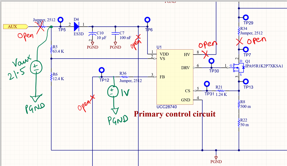
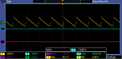
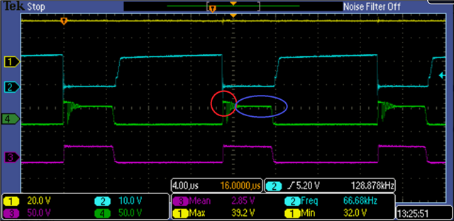
How can I test UCC28740 in an open-loop? I am getting a single pulse at DRV pin when I give 21.5 V at Vaux and no current at the FB pin. I tried giving 1 V across FB pin to feed some uA current but still, the output is a single pulse. How can I get continuous DRV pulses using external power supplies at Vaux and FB? 

Are there any guidelines on using UCC28740 in open-loop?

Thanks,

Nanditha

  • Hi, Nanditha:

    Thanks for asking. 

     It is not easy to use UCC28740 in open loop since it has valley  and line detection. Based on your schematic, auxiliary wilding are open and add a DC source. UCC28740 can not be turned on since there is no input line information and no valley information. Please check the section 7.3.3 in UCC28740's datasheet. It noted all the condition that how UCC28740 generate continuous DRV pulse. It is needed to simulate all the necessary signal, i.e, IVSL, VS...etc. So you may connect MOSFET and aux wilding back, and move 21.5V to C10. Also re-calculate the R5 and R6 based on your input voltage, then UCC28740 could start-up.

    So may I know why you choose UCC28740 to be a open loop PWM generator?  Any feature of UCC28740 is needed?

    If there is no special needs, UC384X series should be easier to achieve the function you need. 

    Regards,

    Wesley Hsu

  • Hi Wesley,

    Thanks for the prompt response.

    I connected all pins of UCC28740 now (except for FB pin) and see that the chip provides gate pulses. However, I see two problems now -

    Channel 1 - VDD ; Channel 2 - DRV; Channel 3 - secondary side output voltage of flyback converter; Channel 4 - Input bulk capacitor voltage

    1. VDD pin max voltage goes up to 44 V if I increase my input (bulk capacitor voltage) > 90 V and then VDD starts to reduce. This cycle goes on. How can I stabilize this? As per the datasheet, the absolute maximum for this pin is 38 V? Is the chip internal circuitry triggering any fault?

    2. With the same setup, if I decrease the load, then the chip is giving only 1 pulse when the VDD has a step change from 20 V to 44 V. 

    Please let me know your thoughts.


      zoomed in plot of pulses

  • Hi, Nanditha:

    Before I share you my thoughts, I would like to explain the start-up process of UCC28740.

    1. In initial stage, no AC input, VCVDD (C7 and C6) is 0V. IC stops. 

    2. Turn on the AC, CVDD (C6 and C7) is charged through HV pin to VCVDD reaches UVLO level (21V).

    3.  The internal switch of HV turns off, IC detects IVSL to check input voltage information. 

    3-1, IVSL does not meet the request level, no DRV signal and IC keep detection till VCVDD decreases to UVLO (7.75V). IC turns off, and HV switch turns on. CVDD is charged again for next cycle. 

    3-2, IVSL meets the request level. DRV ON. Vo increases and transfer voltage to aux wilding (Vaux), Vaux would turn on D4 once Vaux > VCVDD and it provides power to UCC28740.

    According to your waveform, VDD goes to 44V once after DRV signal ON. The output voltage is 25V and VDD is 44V.  This high voltage comes from aux for sure since HV turns off after VDD>21V, and if your R5 and R6 keeps 63.4kohm and 12.4kohm, It triggers IC OVP when VDD is 44V since the Vs.ovp is 4.6V.

    The reason that you may find the DRV pulse is more in regular load than light load is the Vout drops. Since you are using open loop control, Vo is regulated by MOSFET on time and transformer turn ratio. Vout is impact by output loading since no feedback signal to inform IC to increase MOSFET on time to keep output regulation. 

    Lower Vout means lower Vaux. It may delay the OVP trigger timing. 

    Would you please check the turns ratio between Ns:Naux? It seems your turns of aux is too much to cause this high voltage. You may find this spec. on page 5 in datasheet. 

    The calculator of UCC28740 is as below, please use this calculator to set R5/R6 in proper values, also, it provides a transformer design based on your input/output spec. I thought it would be helpful to you

    sluc487

     Regards, 

    Wesley 

  • Hi Wesley,

    My auxiliary to secondary turns ratio is (Na/Ns = 1.18). For an output voltage of 25V, I expect a 29.5 V across the auxiliary winding. I am not sure why VDD goes to 44 V. See below I captured the auxiliary (TP5 to PGND) and secondary winding (TP2 to SGND) voltages when MOSFET is turned on.

    Channel 1 - VDD; Channel 2- DRV; Channel 3 - secondary winding voltage; Channel 4 - auxiliary winding voltage

    I am still trying to understand which protection feature is stopping the gate pulses.

    Thanks,

    Nanditha

  • Hi, Nanditha:

    I have some suggestions according to your transformer design for you reference.

    1st. The turns of Auxiliary wilding is too high. The UVLO(off) is 7.75V. It means we just need to supply the voltage which is over 7.75V from auxiliary wilding, i.e. 12V~15V. It is enough to keep UCC28740 operation. 

    2nd. According to the waveform you shared, sorry it is too small to read the voltage, but it still provides us a useful information. Please check Vaux in red circle. I think the max value is closed to 44V and when you take a look into blue circle, the max value is closed to 29V.

    This waveform shows your auxiliary wilding has a big ringing, which usually comes from VDS of primary MOSFET. Therefore, the CVDD is charged by the voltage ringing in red circle.  That's a reason to make VDD voltage out of design. 

    3rd, What's your value of R5 and R6? UCC28740 senses the output voltage through Vaux. Thus, the VS voltage(in blue circle) is 29V based on your design. If R5 keeps 63.4kohm, and R6 is 12.4kohm, the Vs voltage would be 29V*R6/(R5+R6) = 4.7V, which is over Vovp threshold to trigger OVP. 

    You could find this spec. on page 5 in datasheet, and how UCC28740 senses output voltage on page 14 (fig.13) in datasheet. Thus, if you still keep R5 and R6 value are as the same as the circuit you shared, it's needed to optimize them to make your converter normal operation.

    By the way, there are some the reason to cause voltage ringing, such as higher leakage inductance, long current trace, and transformer structure...etc. Voltage ringing would be lower once they are improved by the design. 

    Regards, 

    Wesley  

  • Thank you, Wesley!

    I adjusted the RS2 value (from 12.4 k to 8 k) and now I see continuous gate pulses for all input range.