Intro
Typically, most ICs are available in industry standard packages such as SOIC and DFN. Even among competitors, many devices are designed to have the same pinout so they can be easily replaced or upgraded. In the last year, there have been supply issues which have led to increased interest in using older devices as temporary replacements. One issue with this is that older devices may not be able to match the performance of newer devices. However, there are some things designers can do to accommodate for these performance differences.
Adjusting for Drive Strength
Newer devices tend to have higher peak source and sink currents. The advantage of this is that it reduces the switching losses in the FET, which is especially important for operating at higher frequencies. The downside is that high currents can lead to noise and ringing on the gate of the FET, especially if the traces and layout are not ideal.

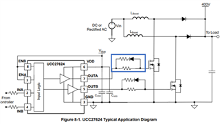
The blue box shows a common layout for gate resistance. The anti-parallel diode and resistor allow for separate configuration of peak source and sink currents. It is highly recommended to set a placeholder for a gate resistor when designing a system so that it is possible to try different resistance values. When selecting a new driver with different source/sink currents, increase the gate resistance to decrease the peak current or decrease the gate resistance to increase the peak current. These documents have additional information about adjusting peak source and sink currents.
Understanding Peak IOH and IOL Currents
Understanding and comparing peak current capability of gate drivers
Thermal and Switching
Some packages, such as DDA and D, are able to be pin-to-pin replacements with each other. The DDA package is simply a D package with a thermal pad that improves heat dissipation. If switching from a D to a DDA package, the thermal performance improves. However, you will not see much improvement over the D package if the thermal pad isn’t connected to a ground plane. If switching from DDA to D, the thermal performance should be checked to ensure that the IC does not overheat.
This equation gives an approximation of power dissipated in the driver. Multiplying PQG by the Junction-to-Ambient thermal resistance (RΘJA) of the chosen package will give a rough estimate of the temperature increase the part will experience. Refer to the “Detailed Design Procedure” section of the device’s datasheet for more information. Section 8.2.2.3 on page 18 of UCC27289’s datasheet has a detailed explanation in particular. It should be noted that these equations are estimates, and other factors such as layout have an effect on the thermal performance. See this document about thermal performance of IC’s:
Semiconductor & IC Package Thermal Metrics
How to Calculate the Max Frequency of a Driver
CMOS vs. TTL
These logic architectures determine what voltage level on the input pins generates a high or a low output. As long as the controller can drive the inputs beyond the threshold voltages described in the datasheet, the inputs will register.
For example, the UCC27289 has TTL inputs, but can accept CMOS type control signals as well. Simply reference the datasheet’s electrical characteristic’s input section:

In this case, as long as the input signal’s high level exceeds 2.4V and the low level is below 0.9V, the inputs should register correctly.
Half-Bridge Only
Bootstrap Circuitry
Some drivers include a built-in bootstrap diode, and others do not. An internal diode reduces the part count of a board but allows less design flexibility. If the previous driver in the system had an external bootstrap circuit, it is possible to simply drop-in a driver that has an internal diode as a replacement. The external bootstrap circuit could be left unpopulated to break the circuit. However, the reverse situation – replacing a driver with an integrated diode with a driver without a diode - will require a redesign to add the bootstrap circuit. Refer to this document about the bootstrap circuitry:
Bootstrap Circuitry Selection for Half Bridge Configurations
Determining Minimum On-Time of Low-Side Transistor
HS Noise
Many applications, especially motors, can have large inductive voltage spikes due to the rapid switching of inductive loads. This noise will appear on the HS pin of the driver and can cause damage or performance issues if large enough in magnitude. All drivers have a certain amount of negative voltage on HS that they can handle without issue, which will be shown in the datasheet. However, if the noise is too great for the driver, other steps must be taken to reduce it.

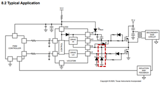
The red, dashed box showing a Schottky diode placed close to the HS pin is common way to reduce noise. If the noise spike exceeds the diode’s forward voltage, the diode will conduct and pull HS towards ground. Ideally, this limits the negative HS voltage to the diode’s forward voltage. Similarly, a Schottky can be used on the LO and HO pins to reduce noise in the same way.
Another method used is the snubber resistor. Placing a small resistor between the driver’s HS pin and the load can reduce the magnitude of noise that appears on HS. The downside is that this resistor is in the bootstrap’s charging path, so it replaces the Rboot resistor and limits charging speed.
Lastly, layout is an important tool for reducing such noise. The HS plane should be large, but overlapping with other planes and traces should be minimized. In addition, it is recommended to separate the signal and power ground planes to prevent ground noise on the outputs from causing issues on the input signals.

