


Other Parts Discussed in Thread: TINA-TI,
Hi Mike,
Thanks for replying, So I guess using the WEBENCH designer is not an option for the above application.
Nevertheless, I have started with the simulation of the design on TINA-TI using the component values as suggested by design note SLUC222D. However, I am not getting the desired results. Here are some of the observations I have made from the simulation
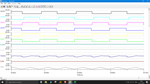
1. Vout is exactly half of the desired output voltage of 84V.
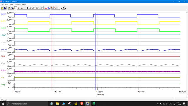
2. I had to decrease the value of the Current transformer loading resistor R1_2 from 12 Ohms to 1 Ohm, otherwise the output would drop below 10V as the Vsense value would rise above 2V (which I guess is the threshold) at which the switching cycle seems to get reduced (perhaps even terminated) resulting into lower output voltage due to reduced duty cycle. After changing the value to 1 Ohm the V_sense stays within 1V. I don't think this is the right solution as it would hamper the peak current limit for the cycle.
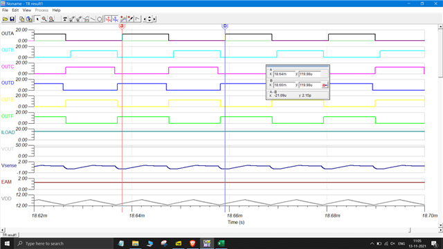
3. The period of the switching cycle is 21u sec as opposed to the desired value of 10u sec (100kHz). I have placed a 121k resistor at Rt pin as suggested by the calculations. let me know if I have made some silly error over here or not.
4. EAM is at 1.25V (as expected due to the gain of the voltage divider and the output voltage). This results in the COMP pin getting saturated at 4.25 volts. EAP is set at 2.5V. The Left and the Right leg Mosfets are overlapping at almost >80% as opposed to the suggested Dtyp of 65%.
5. Shim inductance is kept at 4uH (8uH in total considering the leakage inductance of the transformer) although calculation recommends none is needed. The turns ratio is 3:1 as suggested.
I agree with your point that the efficiency goal has not been reached most probably due to the high values of lossy and parasitic elements. I guess selecting better switching devices and other passives along with a little compromise on efficiency might solve this issue.
I am currently studying the datasheet as to get more details regarding what may be causing the above issue although I would highly appreciate it if you could shed some light as to what might be causing this above issue. I am not completely sure but I feel that the main transformer might not be edited well from my side, please let me know if that's the case or not.
I am attaching the excel sheet calculation and the simulation file at the end. Any help or suggestion is highly appreciated. I will update the post if I get some new insights from the simulation.
Regards,
Jonathan.
5344.UCC28950_PSFB_390_input.TSC
P.S- What does the X parameter in the CESR capacitor in TINA-TI signify ? is it multiple no of that component in parallel or something else.

 Regards,