Other Parts Discussed in Thread: TPS62933
Dear sir:
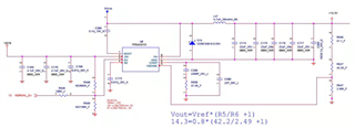
We use tps54331 to design a circuit with an output of 14.3V
Our input power supply is a 4s2p battery pack with a voltage range of 14.4V ~ 16.8V.
The circuit diagram is as follows:
The problem points are as follows:
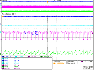
1.When the voltage of the battery pack is above 16.0V, the no-load output is stable and can carry load; When the battery voltage is less than 16.0V, the output is sawtooth wave, which can be stable when the load is about 100mA, and the output drops to 0V when the load is more than 100mA
Does this phenomenon mean that VIN Vout is too small, resulting in unstable output.I tried to add a diode between the input voltage and boot. In this way, the input voltage is less than 16.0v, and the output voltage is also stable, but the load cannot be added. Once the load is added, the output is basically reduced to 0V.
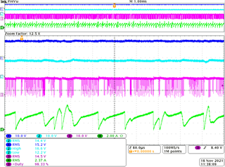
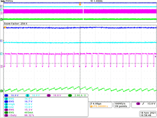
I have measured the waveforms of boot and pH as follows:
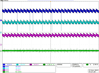
Vin=15.9V ch1:PH CH2:BOOT CH3:VOUT CH4:IOUT
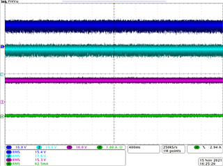
Vin=16.3V ch1:PH CH2:BOOT CH3:VOUT CH4:IOUT
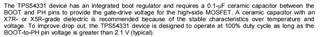
Can tps54331 output stably only when the capacitance voltage between boot and pH is greater than 2.1V?
Can tps54331 output stably only when the capacitance voltage between boot and pH is greater than 2.1V? 14.4V ~ 16.8v input cannot output 14.3v? If you want to achieve 14.3v output, are there any improvement measures?
2.How to implement 100% duty cycle?
Thank you very much!