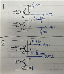
Hello, TI's Team:
Have a nice day.
When we use TL494, we have encountered a question and hope to get your help:
We found that there are two circuit about the output transistors like the below picture,And it make me comfused that the logic of the output duty cycle of these two circuits is not the opposite?
If I apply the circuit 2, would the higher the Vcomp voltage, the greater the duty cycle? If so, shouldn’t the design of the feedback circuit have to be reversed?
Thank you very much.
(PIN 13 is connected to Vref.)


