Hi Team,
There is a good new that we DIN TLV1117DCY!
And there have one thing need your support,
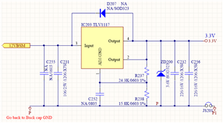
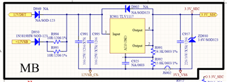
Please help check this SCH, THX
This thread has been locked.
If you have a related question, please click the "Ask a related question" button in the top right corner. The newly created question will be automatically linked to this question.
Hi Team,
There is a good new that we DIN TLV1117DCY!
And there have one thing need your support,
Please help check this SCH, THX


Hi Kygo-san,
I've reviewed the schematics and layout and I have a couple questions.
Regards,
Nick
Hi Nick
After discuss with customer,
1.The out put current is 0.5A!
2.May I know the layout is OK? Does customer need to relayout ? THX
Hi Kygo-san,
12V - 3.3V @ 500mA is 4.35W dissipated in the LDO. This would correspond to a junction temperature rise of over 400C in the DCY package. This is obviously too much power being dissipated. The options they have are to use additional LDOs in parallel to help spread the power dissipation, or to use a DC/DC to get the voltage down before going into the LDO.
To answer your second question, the layout looks fine if there was not so much power being dissipated in the LDOs, but will likely need a relayout because of the issue I mentioned above.
Regards,
Nick
Hi Nick
1. So I need to check below Red frame Junction-to-ambient thermal ? THX
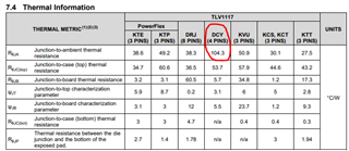
2. And could you suggest a solution for this case ?
And it could meet 12V - 3.3V @ 500mA ,THX
Hi Kygo-san,
Regards,
Nick