Hello,
Please tell me about the following layout questions.
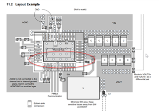
・Why the AGNDSNS should be on another layer?
・If AGNDSNS and the thermal pad are the same layer (surface layer) with a gap of 0.14 mm(0.00551 inches), is there a possibility of noise malfunction?
Is there actually such a case? Can the case be an OVW/OVF/OCF false positive? What is the mechanism?
・Is the return current flowed to the thermal pad as much as GND (PGND)?
Best Regards,
Ryota Shibahara