This thread has been locked.

If you have a related question, please click the "Ask a related question" button in the top right corner. The newly created question will be automatically linked to this question.

UCC27714: HO PWM Top side having slope and LO PWM's Magnitude Reduced

Part Number: UCC27714


Hello TI Experts,

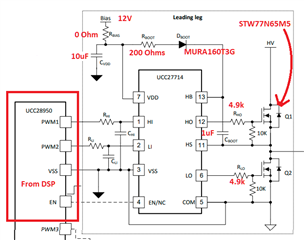
I am Using UCC27714 IC for my Totem pole line synchronous Mosfet Switching. The Resistors and capacitors values are marked in the below figure

The HO PWM obtained is given below

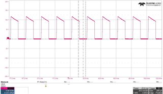
Why there is a slop present in the top side of the PWM ?? also the LO PWM obtained is a perfect square shaped one but do not have the magnitude of 12V

LO PWM

Device Used : STW77N65M5

Diode : MURA160T3G

Switching Frequency : 50Hz (AC Line Frequency)

I am expecting a good support from ur side to sort out my issue !!!

  • Hello Anoop,

    One observation I see is there is a 4.9K gate resistor and 10K gate to source resistor, so there is a noticeable divider ratio from the driver to the MOSFET Vgs. There will be 10K/14.9K x VDD which likely explains the low amplitude on LO. With 12V on VDD there will be only ~8V on the Vgs. 

    For the slope on the HO output there is the consideration of discharging the HB-HS capacitor during the HO on time due to the device IqHB and the current into the 4.9K +10K resistance.

    The current from the gate and Vgs resistors will be ~800uA and the Iq on HB is ~65uA for a total of 865uA. As an estimation assuming the current is constant, Using dV=dt*I/C dV is 10ms * 865uA/1uF= 8.65V. This is higher than in the scope plots but indicates there will be substantial drop from the HO high sourcing current into the resistors.

    To reduce the impact on the Vgs peak levels, review the gate resistor values and gate to source resistor values. If 4.9K gate resistance works well in the application, consider changing the gate to source resistors to 47K ohms. This would result in ~10.9V Vgs with 12V VDD. 

     To further reduce the HO output level dropping, I would suggest trying a 2.2uF HB to HS capacitor. That change with the 47k Ohm Vgs resistor will reduce the discharge of the HB to HS capacitor.

    Confirm if this addresses your questions, or you can post additional questions on this thread.

    Regards,

  • Hello Richard,

    Thanks for your valuable suggestion. I have one more doubts regarding this. The Rboot used here is 200 ohms. Does this resistor only serve the purpose of Current limiting agent for Dboot ? or it have any other impact on my circuit operation. ?? My working freq is 50Hz only. but when i raised the freq to 10kHz i didnt get the output. 

  • Hello Anoop,

    Since you had mentioned the operating frequency was 50Hz, I did not comment on the boot resistor value. The boot resistor size is to limit the peak current in the boot diode and also control the rise time of the bias during startup. With 200 Ohms and 1uF boot resistor and cap the time constant will be very long at ~200us. That would be an excessive charging time for 10kHz operation and may not allow the HB bias to rise. For 10kHz assuming 50% duty there would be ~50us low side on time. I would allow 3 time constants to achieve close to full charge which would be ~ 16 Ohms. 

    Also to determine the minimum boot resistance I would target ~20us HB rise time, assuming 3 time constants this would be ~7 Ohms. Also make sure the boot diode peak current rating is at least VDD/Rboot.

    Regards,