This thread has been locked.

If you have a related question, please click the "Ask a related question" button in the top right corner. The newly created question will be automatically linked to this question.

TPS562200: Output current is oscillating

Part Number: TPS562200

Hi,

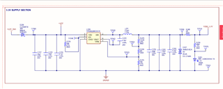
I have used TPS562200ddcr to convert my 12VDC to 3.3VDC. 

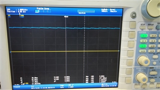
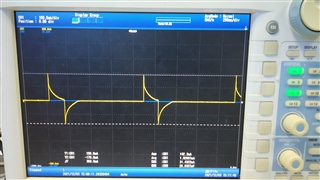
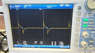
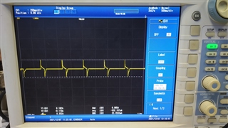
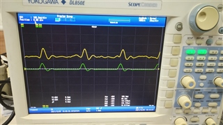
While testing the module on my PCB I noticed that I receive the appropriate 3.3V output as desired but the output current seems to be oscillating and reaching a negative value which is not ideally the response I was looking for. 

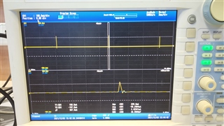
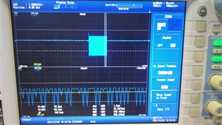
I simulated the same on WEBENCH designer and the waveforms do not match. I am adding an image for reference. The yellow channel is the current.


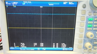
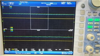
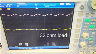
Furthermore, I mounted the entire circuit provided in the product's datasheet on a bare PCB. I added a variable load of 0-100 ohm at the output side.

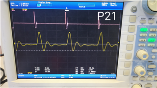
There still seems to be a ringing with the current going below the 0A threshold level. I am adding another image as a reference.


Can the concerned help me qualify this behavior of the IC? 

Thank & Regards

Soham Ranade

Larsen and Tuobro Technology Services 

  • Hi, Soham Ranade!

    According to the waveform of the node SW in first picture, it is normal.

    It may be caused by the testing methods. Please check the following items.

    (1) Is the AC mode open when testing the output current using the CH1 of the scope? 

    (2) Please check the range is appropriate when observing the load current in scope.

    (3) Which way you used to test the load current? Did the current probe be corrected before testing?

    (4) Please check the current probe is locked and the wire connecting the load pass through the current probe reliably.

    And please provide following information to help analyzing your problem.

    (1) Please provide more information about the electric paraments, the schematic, PCB layout .

    (2) Please provide the waveforms of the output voltage, current through inductor in the same operation condition of the two pictures and  the waveform of the output voltage, inductor current in no-load condition.  

    (3)Please provide more information of the characteristic of the load.

    Regards

    BSR-MV

    Shuai

  • Hi Shuai Fan,

    I was partially relieved to know that this behavior of the IC is normal. Thank you for the same. 

    I shall try to answer most of what you have asked for hoping that it helps you to get to a concrete solution. 

    (1) Is the AC mode open when testing the output current using the CH1 of the scope? 

    If by AC mode you mean the AC coupling enabled on my scope, then yes it was set to AC coupling initially and later I also switched it to DC coupling but obtained the same response. 

    (2) Please check the range is appropriate when observing the load current in scope. 

    Both my TektronixA261 current probe and my scope were set in 1:1 setting initially. Then in order to magnify the output I changed the ratio by a factor of 10. The waveform named P21 is this amplified output. 

    (3) Which way you used to test the load current? Did the current probe be corrected before testing? 

    The direction of my scope was set as per the guidelines given in its datasheet. Unlike other Current probes, this particular one does not require/ has a knob for ZERO adjustment setting. It was also calibrated leaving very less room for error

    Attaching a picture here for direction reference. 


    (4) Please check the current probe is locked and the wire connecting the load pass through the current probe reliably. 

    I do not clearly understand what you mean when you say that the current probe should be locked. As far as the wire is concerned, I took into account the wire length along with the gauge required for the approximate current consumption. Hence things were reliably placed. 

    (5) Please provide more information about the electric paraments, the schematic, PCB layout 

    I am adding in the screenshots of my schematic and PCB layout. In most cases I have tried to cover the Top and Bottom Layers along with the Power Supply line. I hope these images help. 


    1. Schematic 

    2. Bottom & Power Layer 


    3. Top & Power Layer 


    4. Vin 


    5. GND/Vss 


    6. Inductor Output side 


    7. Load

    (6) Please provide the waveforms of the output voltage, current through inductor in the same operation condition of the two pictures and  the waveform of the output voltage, inductor current in no-load condition.  

    I shall provide these tomorrow or day after as I need to be present at my lab to obtain some of these. 

    (7)Please provide more information of the characteristic of the load.

    In the 32ohm load.png file, the load used is a  (0-100Ω) 5% , 300W rheostat 

    As for the P21 image, I cannot say much as that contains some proprietary information on the main parts of my circuit. 


  • Hi, Soham Ranade!

    Thanks for your information. Have you tested the current of other circuit by the same current probe and the same testing method?  At present, your problem is still doubt as a matter of measurement.

    Actually, for a switching DC-DC converter, the output voltage has some AC ripple in normal. But it is very small, about mV level. When loading a resistor, if the scope is set to 5V/div and DC coupled , the output voltage will be look like a smooth DC, if it is normal. So as the output current.

    Waiting for your waveforms of the output voltage. the voltage of node sw, the current through inductor ,the output current. All of them need to be tested in no-load condition and the resistor-load condition with DC coupled setting.

    Regards

    BSR-MV

    Shuai

  • Hi Shuai Fan

    I have used the same current probe(TektronixA261) and testing method throughout. I even verified things for repeatability using TektronixA622 and found the same results.

    Below you shall find all the waveforms. Please do point out if I have missed out on anything or if you need any other waveforms as well.

    Voltage Waveforms are in Blue while Current in Yellow. When one channel is being used, the other has been kept on to signify zero position.


    1. 3.3V output @ no load 


    2. 3.3V output @ 14.5ohm resistive-load

    3. SW (Pin2) at no load is same as 3.3V output @ no load 


    4. SW Output Voltage at 14.5ohm load


    5. SW output at 30ohm load (extra waveform added)


    6. Current output at 14.5ohm load (1) 


    7. Current output at 14.5ohm load (2)  


    8. Inductor Current at no load

    9. Current through inductor @14.5ohm load. 

    Thanks & Regards,

    Soham Ranade

  • Hi, Soham.

    1.Please provide the current scale of CH1 ,?A/div. For 3.3V Vout, the current OF14.5ohm is about 227mA. and you can set the scale at 200mA/div.

    2. The frequency of the output voltage ripple and the frequency of the SW should be the same, if it is normal. Please use the same time scale. About the no-load, the frequency of the output voltage ripple is about 8ms. But the frequency of SW in picture.3 is seems 8us. Please double check it.

    3. In your waveforms, the output voltage is a good DC voltage. For a resistor load, the out put current should also be a good DC current. I can not understand it, why it shows a AC waveform in picture.6 and 7. Can you testing the output current by another current probe. If the problem is caused by a bad probe, by changing a good one, it may be solved.

    4. Can you take a physical picture which shows the position of the current probe and the wire of the load current which pass through the current probe? If there is another wire which is closed to the current probe, it may cause disturb.

    Shuai

  • Hi Shuai Fan,

    I shall try to answer your questions in chronological order. 

    1.Please provide the current scale of CH1 ,?A/div. For 3.3V Vout, the current OF14.5ohm is about 227mA. and you can set the scale at 200mA/div.

    The current scale is at 100mA/div in the previous screenshot. As per your request, I have added in the screenshot where the scale is set at 200mA/div for a 14.5ohm load. 


    2. The frequency of the output voltage ripple and the frequency of the SW should be the same, if it is normal. Please use the same time scale. About the no-load, the frequency of the output voltage ripple is about 8ms. But the frequency of SW in picture.3 is seems 8us. Please double check it.

    For ease of understanding, the 3.3V output voltage and SW waveform are plotted on different channels at the same time. CH2 is SW o/p and CH9 is o/p voltage . Both have same frequency. I have zoomed in and adjusted the position to make it properly visible.

    As you said earlier, time period is 8ms for both.


    3. In your waveforms, the output voltage is a good DC voltage. For a resistor load, the output current should also be a good DC current. I can not understand it, why it shows a AC waveform in picture.6 and 7. Can you testing the output current by another current probe. If the problem is caused by a bad probe, by changing a good one, it may be solved. 

    The probes I am using are calibrated recently. To cross check I checked the same using a 40V,50Hz line across the 14.5ohm load and found the current to be 2.75Arms. 

    I have plotted the DC current using 2 different current probes on the same screen. Hope that helps.

    In the first screenshot the load is 14.5ohm while the second is using my primary circuit. 


    4. Can you take a physical picture which shows the position of the current probe and the wire of the load current which pass through the current probe? If there is another wire which is closed to the current probe, it may cause disturb.

    I have taken the picture from 2 different angles for ease of visibility. I even tried increasing the no.of windings around the clamp for increased sensitivity but again found the same results.  


    Thanks & Regards,

    Soham Ranade

  • Hi,Soham Ranade!

    1.From your picture, the load wire is to long , it may increase parasitic inductor and bring disturb. It suggest you use a short wire between output cap and the load resistor.

    2.From your picture, the hole of the current probe is far large than the load wire, it is possible that the probe can detect the magnetic field sourced by the load current. It suggests to use a current probe with a small hole for measuring a small current, such as the following picture. 

    3. It suggests you test the voltage of the resistor directly , which don't conclude the impedance of the load wire.

    4. You tested an AC current with your current probe. But your target is DC current. How about result of testing a DC current?

    Regards

    Shuai

  • Hi Shuai, 

    1. I reduced the wire length significantly (down to few centimeters), but I did not observe any significant change

    2. I used a Tektronix A622 which is has the smallest range as 100mV/A. The probe is very similar to the one you have shown here. Also it is a AC/DC current clamp as opposed to the A621 which is purely an AC Clamp. 

    Unfortunately I had to reduce the bandwidth down to 50kHz to get a noise-free response. You can have a look at the same in the attached screenshot. The one in yellow is the AC/DC clamp's waveform. 

    Lastly, I do not have a pure DC clamp if that is what you suggested on using. 


  • How about the waveforms on the resistor?

  • Hi Shuai Fan,

    I was unable to test the last part since I was busy with some board modifications.

    Since there was a shortage of the IC and I was unable to qualify the current behavior, it was decided to go ahead with an LDO instead.

    I shall continue to run the tests later sometime, but in the meantime I shall close our loop by addressing this issue as ''Resolved"

    Thank you for your time and patience. I appreciate the help. 

  • Hi, So Ra.

    For your application, the 12Vin to 3,3Vout. If using LDO, the efficiency will be bad, because the large difference between input voltage and the output voltage. The low efficiency will cause a bad thermal.

    Shuai.

  • Hi Shuai,

    I tested my system for around 6 hours, fortunately the heat dissipation is not as severe. 

    So for the time being I am going ahead with the new modification,. 

  • Hi So Ra!

    Best wishes!

    MV

    Shuai

  • Thanks,

    Happy Holidays!