This thread has been locked.

If you have a related question, please click the "Ask a related question" button in the top right corner. The newly created question will be automatically linked to this question.

TPS546C23: About the Vds waveform when CNTL pull down

Part Number: TPS546C23

Hi team,

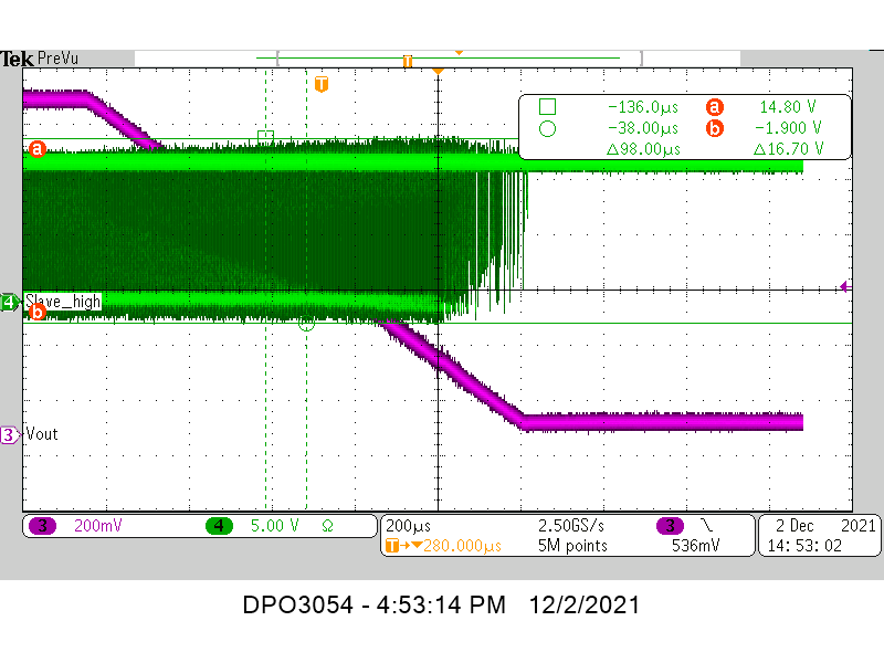
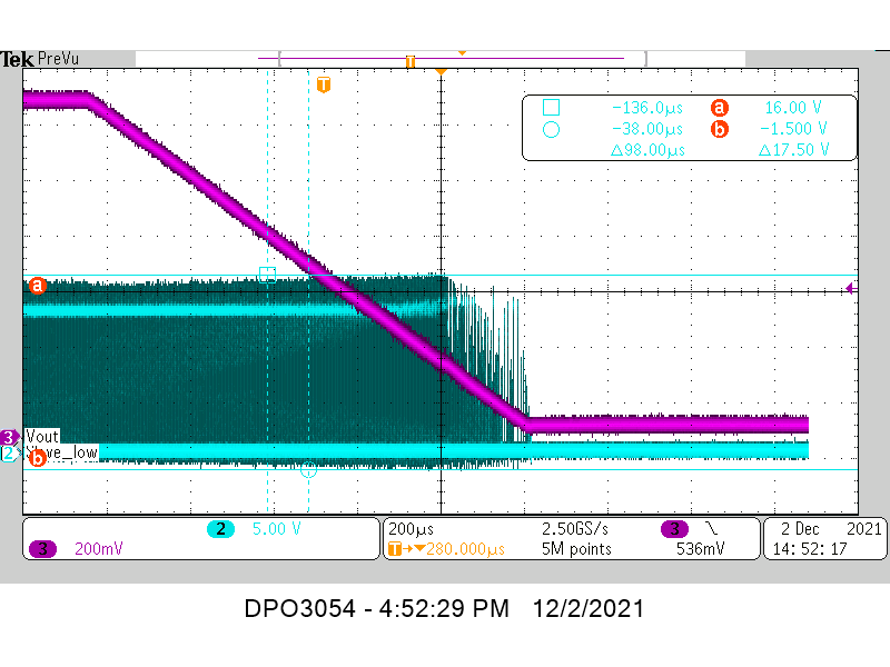
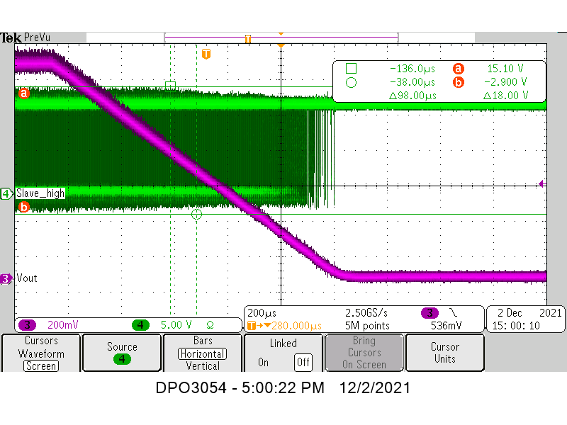
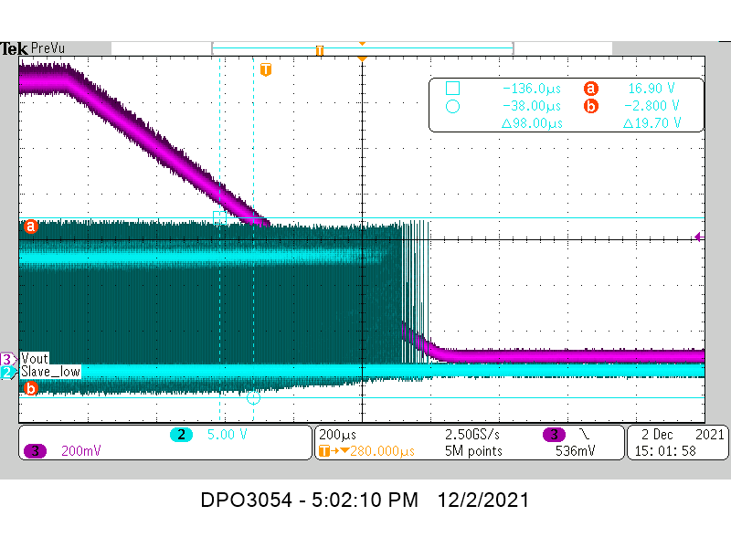
I test the TPS546C23EVM, control the CNTL pull down to disable the output of TPS546C23, and test the Vin to SW(High Mos Vds)

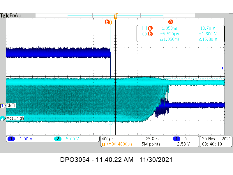
Seeing that the output has a soft shutdown of 1ms, and the 500us Vds has also increased in the end, so I want to confirm what our soft shutdown control mechanism is, and why the High Mos Vds will increase?

Best regards,

Andy Liu

  • Would you mind adding the VOUT waveform to the plot? Also, what kind of load is it? Is it a resistive load?

  •  

    The TOFF_FALL control of the TPS546C23 keeps the switching converter operating while the reference voltage is decreased from the regulated output voltage to 0V over the period of time defined by TOFF_FALL.  For 1ms, that means forcibly discharging the output voltage from Vout to 0V over 1ms.

    The increased Vsw voltage during the decrease in VOUT is most likely caused the output capacitor discharge current (Vout x Cout / TOFF_FALL) exceeding the load current, resulting in a negative inductor current.  The negative inductor current causes the dead-time current to flow into the SW node from the inductor and through the body diode of the high-side FET rather than out of the switching node into the inductor through the low-side FET.  The drop across the high-side body diode during this dead-time increases the voltage on the SW node.

    Peter James Miller 

  • Hi Miller,

    The waveform tested yesterday was wrong. I tested the Vds of the High Mos but used a longer lead, which introduced interference, so the picture is wrong;
    Please refer to the following two figures, which are the High Mos Vds and the Low Mos Vds. Figures 1 and 2, there is no load when disable the device. You can see that the Vds of both High Mos and Low Mos have risen. Could you help explain the reason for their rise? Especially the High Mos Vds, I saw a rise of about 1V;

    At the same time, the figure below shows a 40A load, and then disable the device. You can see that the highest value of the High Mos Vds has dropped, with the duty cycle is slowly decreasing; And the lowest value of the Low Mos Vds,  the negative pressure of SW is also somewhat decrease, the duty cycle is gradually reduced; how can I understand here? It seems that when disable the device, there is or no load, the state is different. Please help me to solve the confusion, thank you.

  •  

    What you are describing is the same phenomena that I described before, with some additional details.

    When the inductor current is zero amperes average the Peak inductor current, when the high-side FET turns off, is positive and the inductor draws current out of the switching node until the low-side FET body diode conducts current, forcing a negative voltage on the switching node.  When the low-side FET turns off at the valley current, the valley current is negative, and the inductor drives current into the switching node until the high-side FET body diode conducts current back to PVIN, resulting in a peak SW voltage greater than PVIN.

    When the converter is disabled with a 1ms soft-stop timing and over 2,000μF of output capacitance charged to 3.3V, the average inductor current is forced negative, driving more current through the body diode and charging up the VIN capacitors, increasing the VIN and SW voltages.

    However, when the converter is delivering 40A of current, the 7A of current needed to discharge the output capacitors does not result in negative inductor current, just less positive inductor current.  The converter only needs to deliver 33A of current instead of 40A of current.  The lower current produces less ringing and lower switch node voltage stress.