


Hello,
I have a question regarding pad spacing, high-voltage, and IPC-2221:
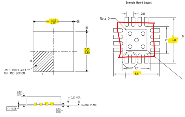
Regarding spacing between pins 7 (SW) and 8 (GND) of the QFN package. If I take some measurements from the package diagram:
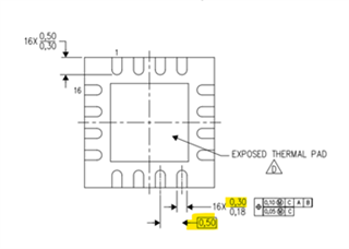
- Pad width = 0.3mm (max)
- Pin-pitch = 0.5mm (nominal)
- Gap in between pads = 0.2mm (min)
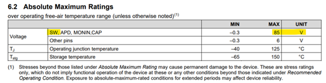
Per the TPS61391 ABS max table, the maximum voltage between these two pins can be 85V:
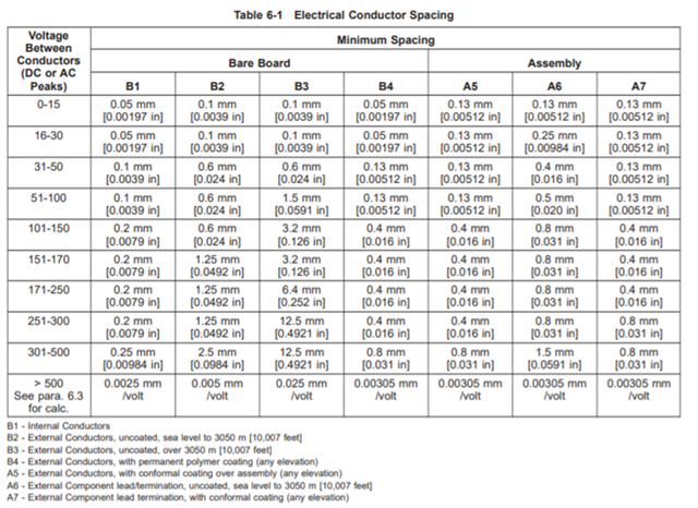
Per the IPC-2221A (link below), the minimum spacing between these pins is 0.5mm:
The recommended land-pattern in the datasheet suggests that we extend the pads beyond the package ends (red box approximates where the package will sit on the recommended land pattern)
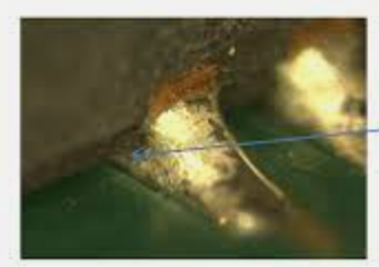
Since the lead-frame of the package extends up the sides, there will be a solder fillet in the final assembly like so:
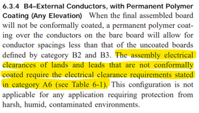
Given the clearances dictated by the package mechanicals combined with the higher voltages involved. What's the recommended strategy if we need to be compliant with the IPC-2221A spec? Conformally coating seems to be the only option here. If so, conformal coating is not a technology conducive to products that integrate APD's (like optical modules). Are there any other ways to make this work?
Don
