A related question is a question created from another question. When the related question is created, it will be automatically linked to the original question.
If you have a related question, please click the "Ask a related question" button in the top right corner. The newly created question will be automatically linked to this question.
LM5069: LM5060 - Alternate Part for LM5069MM-2/NOPB
Part Number: LM5069 Other Parts Discussed in Thread: LM5060
Hi Team,
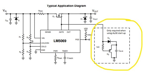
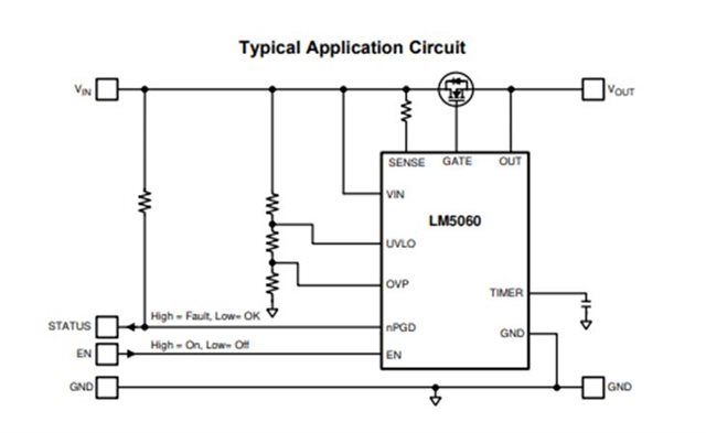
On the alternate LM5060, can the dv/dt circuit be included for the MOSFET as in LM5069 as a support to Hot swap feature. Please refer the below figures.
Thanks for the feedback. We have further one clarification to be made :
We are looking for the alternate to LM5069MM due to OV Spikes & UV Glitches so the alternate part search is LM5060. Also we would need to know if LM5060 overcomes such issues as in the LM5069MM. Need your advice and Recommendation.
We are using I/O Cards as hot plug to Hot Swap Controller and avoid inrush issues.
On full load the in-rush current protection circuits of LM5069-2 IC gets activated before the system reaches stable nominal voltage of 24V DC. This causes a reboot of the IC and thus rebooting the entire device making it unstable.
In real time applications the fed input power causes voltage spikes or voltage dips for a few milliseconds in turn falsely triggers the OV/UV protection circuitry of LM5069, therefore leads the system reboots needlessly.
We plan to use LM5060 but will the same problem appear in this IC also.
We need to enable the load using PG signal of LM5069 else the circuit starts in power or current limit mode and fails to start. Can you fill LM5069 design calculator with your inputs to check external parameters. It is available at LM5069 Design Calculator (Rev. D)
For OV Spikes & UV Glitches issues, use capacitors at EN/UVLO and OV pins to avoid system reset
Could you please review the Circuit been designed for application.
1. The Input Voltage is, Min19.4V and Max 29.5V , and we are expecting any voltage glitch under 19.4V should be treated as UV and any spike above 29.5V should be considered as OV with a Typical O/P Voltage of 24V at Max 12A rating.
2. As already mentioned above there are 2 current issues which triggers falsely for System Reboot.
3. Yes we have added additional capacitors EN/UVLO and OV pins