This thread has been locked.

If you have a related question, please click the "Ask a related question" button in the top right corner. The newly created question will be automatically linked to this question.

UCC28740: UCC28740 Power Supply Problem

Part Number: UCC28740
Other Parts Discussed in Thread: TL431

Dear all,

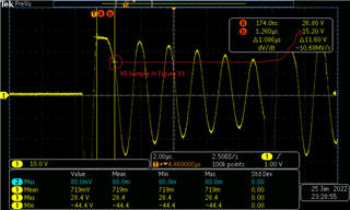
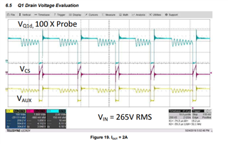
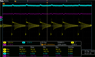
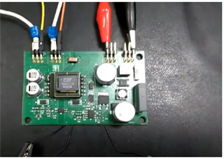
In my project, we are testing a power supply with 3V3 and 2,5A on output circuit.  

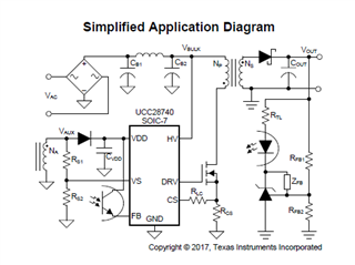
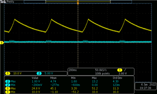
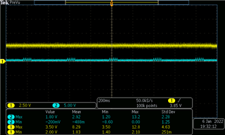
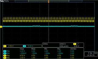
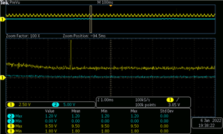
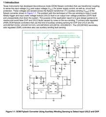
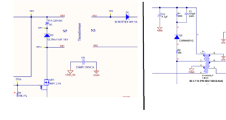
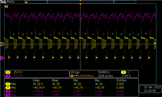
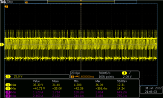
Therefore, the circuit is not switching and we don´t know what is the problem.Following, I am attaching the pictures on testpoints and your measurements. Can technical support help us?

TestPointsPowerSupply.pdf

Thank you very much.


  • Hello,

    I reviewed your waveforms and it looks like VDD is cycling between VDDon and VDDoff.  This would indicate the design is not starting up due to a fault.

    The following application note discusses how primary side fault sensing works and the most common issues with this technique and how to resolve them.  The UCC28740 has this fault sensing technique and this application note should help you resolve your issues.

    https://www.ti.com/lit/pdf/sluaac5

    Regards,

  • Hello Mike,

    Thanks for your feedback.

    I already calculate: Vin(run)=117V and Vin(stop)=41V and I am applying 311Vdc on the Vin pin. Therefore, I still have this fault problem. But, if I lower the value of RS2, the value of Vout will rise. Do you think this can prevent OVP protection?

  • Hello,

    If it is not input under voltage then most likely your note starting up do to ringing on the aux winding trigging OVP or resetting UVLO.  Those faults if they are false can be removed by an RCD clamp on the primary and a snubber on the output rectifier.  The application note covers how to resolve both of those issues.

    Regards.

  • Hello,

    Do all tests need to be done at full load or can I do it in open circuit?

    Regards.

  • Hello,

    Your design should have a pre-load resistor on it that draws 2 to 3 mA.  Besides that the design does not have to be loaded.  

    Regards,

    Mike

  • Hello,

    QUESTION 1: Using this formule,  
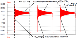
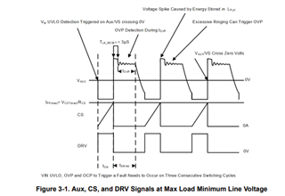
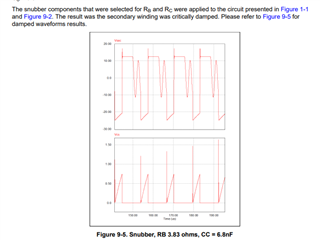
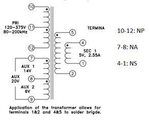
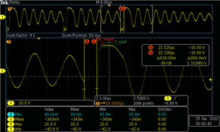
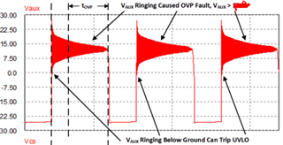
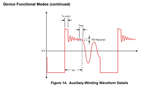
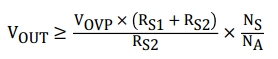
, I have RS1=59k and RS2=68,1k, NS/NA=0.375, because in my project, I design my circuit to operate with 3V3 in outuput voltage (VOUT). Then, using this values resistors, I have Vout>=3,21V. In this context, according to the figure below, my converter was designed to trigger OVP fault protection when VOUT and VAUX  were greater than 3,21V. Is this statement correct?

    QUESTION 2: During switching (permanent regime) we have VDD=VOUT*NS/NA=3.21*NA/NS=8.56V (powered by VAUX). 
    This value is greater than VDDoff (7.75 V from the datasheet).

    Are both questions correct?

    Thank you!

  • Hello,

    The OVP trip point I believe is 4.6V so the OVP on the VS pin.  The control voltage on VS should be 4.06V.

    Vout would be controlled to (4.6/68.1)*(59 +68.1)0.375 = 3.21V.  You are correct your OVP trip point is too low and so is your VDD.

    You are correct.  So you need to adjust your OVP so it is not tripping at such a low voltage.

    Regards,

  • Hello,

    But I designed my power supply to have 3V3 output. 
    So if I increase the OVP voltage consequently I will also be increasing the output voltage.
    But I don't want to do that, because I want to have 3V3 on VOUT. This doesn't make any sense. So how can I design a power supply with 3V3 on the output and not have such a low OVP? It makes no sense!

    According to this formula VDD=VOUT*NS/NA=3.21*NA/NS=8.56V, I have 8.56 in VDD, so it's not that low. 
    I confess that the submitted document is very confused.
    How can I adjust OVP level?
  • Hello,

    The UCC28740 uses a TL431 feedback which should should set your output voltage.  RFB1 and RFB2 set the output voltage.  RS1 and RS2 set input UVLO and OVP.  So you need to adjust your OVP trip point with RS1 and RS2 and not RFB1 and RFB2.

    Regards,

  • Hello,

    I changed the RS2 value to 33k (the last value was 68.1k).
    NA / NS = 2.667;
    NS / NA = 0.375;

    I have  VOUT>=(4.6/33k)*(59k +33k)0.375 = 4.81V. The flyback converter shuts down if VOUT for three consecutive
    switching cycles is greater than 4.81 V triggering OVP protection.

    Now,
    Reflecting on VAUX, we have VAUX = NA/NS*VOUT = 2.667*4.81 = 12.82V.

    Therefore, I still have this fault problem.

    Is this calculation correct?

    Looks like it's not a OVP problem either.

    Is there another alternative I can try? Maybe further reduce the RS value: using RS=10k.

    Thanks.


  • Hello,

    Can you clarify?   The fault calculation is correct.

    If VS is greater than 4.6V during the transformer Demagnetization time for three consecutive switching cycles this will trigger OVP. 

    You need to look at the CS, VDD, VOUT and the voltage across VS resistor divider with an oscilloscope.  That last three pulses before VDD discharges.  This will help determine which fault is being tripped. 

    Regards,

  • Hello,

    Please see the figures below.

    Figure 1: C
    hannel 1 is VDD pin and channel 2 is DRV pin.


    Figure 2:
    Channel 1 is CS pin and channel 2 is DRV pin.


    Figure 3:
    Channel 1 is VS pin (between RS2 and ground) and channel 2 is DRV pin.


    Figure 4: Zooming in figure 3 - Channel 1 is VS pin (between RS2 and ground) and channel 2 is DRV pin.
    Can you find any abnormality in these figures?
    This voltage peak on Figure 4 is always occurring on the VS pin. 
    Do you think the problem might be this? If that's the issue, how can I resolve this issue?
    Just remember, the circuit is not switching and it was
    designed to operate at 3V3 output voltage.
    Thank you!
     
  • Hello,

    You need to look at the switching waveforms before shutdown with higher resolution to see why you are shutting down.

    Problematic aux winding noise causing issues.

    Snubbing and RCD clamp will clean up the aux waveforms. Application note SLUAAC5 gives details on how to evaluate and resolve fault issues.  

    https://www.ti.com/lit/pdf/sluaac5

    Most common issues are aux noise that can be resolved with and RCD clamp and a snubber across the output rectifier.  Those circuits are highlighted below in green.

    Regards,

  • Hello,

    But How can i do it if my circuit IS NOT SWITCHING.

    If it IS NOT SWITCHING, I can not to verify your questions.

  • Hello,

    The UCC28740 gives three sample pulses when it reaches VDDon at the maximum switching frequency if fault is observed it will stop switching.  Trigger on the DRV output and you should see these pulses.

    Look at figure 4-1 in the application note I referenced.  It discusses the three sample pulses.

    I reviewed your schematic and you are using a TVS clamp instead of an RCD clamp.  If you don't have one add a snubber across the output rectifier.  Most likely you are shutting down due to an OVP or UVLO.   The application note reference reviews this in detail.    This application note generally will resolve 98 to 99% of these issues.

    Regards, 

  • Dear Mike,

    There just was another problem.

    When I just removed R6 resistor,  the UCCC28740, the fuse input and R12 resistor burned out. Could you tell me what might have happened?

  • Hello,

    Not sure why you had to remove resistor R6.  The R6 resistor 10 k ohms from gate to ground is just to ensure the FET stays off during power up.  Designers have been doing this for years.  This was because older devices use to come up with the driver high impendence years ago.  It is still a good practice to have that resistor.

    So if you removed R6 and the fuse opened up.  Chances are the gate of the FET may have gotten shorted to a voltage that had driven the FET on at 100% duty cycle.  I would suggested replacing the fusible resistor, FET, UCC28740 and CS resistor.  Also check all the other components in the circuit to make sure they are not damaged.  You should be able use an ohm meter to do this.

    Regards,

  • Dear Mike,

    Thank you for your feedback.

    I have a new quetion. Here we go:

    I have NA/NS=0.375 ration on transformer (NS/NA=2.667).

    Then, VOUT>=[4.6*(59k+68.1k)/(68.1k)]*0.375= 3.21V. This is my voltage protection (OVP).

    In this context, when VOUT is 3.21, I have VDD=VOUT*NS/NA=3.21*2.667=8.56V.

    The VDDoff  maximum value is 8.15V.

    QUESTION 1: The VDD value is very close to the VDDoff value when I have 3.21V on the output. This can be a big issue?
    How can i solve this problem?
    Remember, I project my circuit to operate in 3V3 on output.

    QUESTION 2: During switching, should the VDD value always be greater than the VDDoff value? How much?

    QUESTION 3: In Figure 1, I have VDDoff=9.2V. But, in datasheet, we have VDDoff=8.15V (7.75 V typical). What do you tell me about this? Do we have a problem? Because VDD=8.56V, this is a value below the value shown on the oscilloscope. 

    Thank you.

  • Hello,

    If your output voltage is set for 3.3 V your OVP trip point should be for roughly 15% higher at 3.8 V roughly.  You will need to adjust your VS resistor divider of the aux Winding.

    Question 1:

    You are correct your NA/NS turns ratio is not correct for your design.  If your turns ratio of your transformer is NA/NS = 2.667 when regulating the Vaux would be 3.3V*2.667 = 8.8V.  I would adjust the turns ratio so VDD nominal would be roughly 12V.

    VDD/Vout = 12/3.3 = 3.636 = NA/NS

    Question 2:

    VDD nominal when the flyback is delivering power should be > greater than VDDoff.  I recommend setting it to 12V.

    Question 3:

    The data threshold for VDDoff is correct is a tested parameter and should have a range of 7.35 to 8.15V.  Not sure why you are measuring 9.2V.

    You might want to double check this just to see.  Zoom in on the valley and measure this direction at the VDD pin.

    There is an excel design tool you can find at the following link that you can use to check your design as well.

    https://www.ti.com/lit/zip/sluc487

    Regards, 

  • Hello, Mike,

    I forgot to note one thing.
    See that we have a diode D1 in the circuit. Its voltage drop must be considered.
    So, we have VDD=(VOUT+VF)*NA/NS=(3.3+0.55)*2.667=10.3V.
    VDD nominal, when the flyback is delivering power, is 10.3V. Is this value correct to VDD pin in
    permanent regime
  • Hello,

    You have an aux winding diode.  They should cancel each other.

    Regards,

  • Hello,

    For example, 
    If I don't change the transformer, I can change the output voltage value to 5V output. So, we have VDD=2.667*5=13.3V and RS2=4.6*59k/(2.667*5.75-4.6)=25.3k Could this be a good alternative?
  • You can do that

  • Hello,

    I have another question.

    See the figure bellow.

    On the left we have my circuit, on the right a circuit found on the texas website.
    Question: Some designers do not consider the TVS diode (D2), see the figure on the left. 
    Could you please tell me why the designers don't consider this TVS diode?
  • Hello,

    The circuit on the right is an RCD clamp.  The circuit on the left is a transient voltage suppressor (TVS) clamp (D2).  There are high voltage Zener type diodes that are specified as TVS (D2).  You can find TVS diodes at most of your semi conductor suppliers.


    Regards,

  • Hello,

    Can I remove diode TVS (D2) and add an RCD clamp? Just for a test.

    Regards,

  • Hello,

    Both should protect the FET from an over voltage.  The application note that I sent you shows that the RCD clap is preferred.  Putting a TVS across the R and C in an RCD clamp can be done for safety. 

    https://www.ti.com/lit/pdf/sluaac5

    Regards,

    Mike

  • Hello,

    See the figure bellow.

    This figure is the transformer we are using.

    When we chose this transformer, we thought that the voltage on VDD should be: VDD=Vin*NA/NP=311*0.114=35V. 
    When Vin_rms=220Vac. But in the docs, you don't use Vin, you use Vout to check VDD voltage in permanent regime: VDD=Vout*NA/NS=3.3*2.667=8.8V
    Why do you use the second option?


    Regards.
     
  • Hello,

    This is a flyback the aux winding should be the same polarity as the output that is why it uses Vout to calculate VDD.  Your calculation is actually the negative voltage on the aux winding when the switch is on.  When you check VDD with a voltage meter or scope probe it should varify the VDD calculation based on vout and Na/Ns turns ratio.

    Regards,

  • Hello, thank you for your feedback.

    But I have a many quetions. See the figure bellow. We have a TLK_Reset and T_OVP representations.

    Figure 1; TLK_Reset and T_OVP representations.

    Figure 2: Yours documents.

    My circuit is not switching yet.

    I designed my circuit to operate at 5V at steady state output. 
    When there is an overvoltage, we would have 5.75V at the output. The transformer's transformation ratio is NA/NS=2.667; NP/NA=23.33;

    I designed the circuit to operate at 5V at steady state output.
    I considered an OVP protection voltage at 5.75V.

    Then, we have VDD=5*2.667=13V on permanent regime.

    Your calculator excel doc give to me R1=59k and R2=27k.

    But, look at the Figure 1. We have em T_OVP 25V on Vaux. So VS=25*27k/(59k+27k)=7.85V So VS>VS_OVP. But if I adjust the RS2 value to solve the OVP problem, I will change the protection voltage at the output.
    Question 1: How can I proceed in the best possible way?
    I don't understand why I'm measuring 25V in Vaux.
    Question 2: It should be VS Sample = (Vout+VF)*NA/NS=(5+0.55)*2.667~=15V. Is it correct? Look at next figure for it. 

    Question3:
    in figure 3 which point represents VS Sample in figure 13? Point 1 or 2?

    Figure 3
     
     
  • Hello,

    TLK_RESET is a blanking time and you will not check for OVP at that point.  You will check for OVP after TLK_RESET times out to the sample point.

    Please note TLK_RESET.  Page 14 and 15 in the data sheet escribe how TLK_reset could be 600 ns to 2.2 us based on the primary peak current level.

    I did post the information below but was unable to improve the resolution.  However, you can go do the data sheet to see the same information.

    https://www.ti.com/lit/ds/symlink/ucc28740.pdf 

    If your output voltage is not coming up during the dmag time the aux winding should not be reaching 25 V.  Maybe the polarity of your transformer connections is not correct or your turns ratios is off.  Because Vout*Na/Np should roughly be Vaux during the dmag time. If Vout is zero the voltage at vaux + should not be 25V during the dmag time.  It should be closer to 0 volts.

    Double check the transformer turns ratios Np/Ns and Na/Ns secondary to make sure they are correct as well.

    In regards to your figure 3 the waveform does not look correct.  The resonant ring should be uniform and should resemble figure 13.

    The waveforms below came from a working a design  

    Your waveforms the sample is taken at 1.  Not sure what is causing waveform between points 1 and 2.  I wonder if something is breaking down in your design causing the output voltage to deplete.

    I would suggest probing Aux, CS, and the secondary winding and output voltage during this behavior.  Maybe it will help identify what is breaking down.

    There is also an evaluation module for the UCC28740 that you may find useful.  The following link will get you to the User's guide for the evaluation module.  There are critical waveforms in the user's guide that you can evaluate to see what they are supposed to look like.  It also gives a schematic and the layout for the design as well.

    https://www.ti.com/lit/ug/sluual8/sluual8.pdf

    Regards,

    Mike

  • Dear Mike.
    My circuit is working perfectly. All voltage levels are correct as described in the datasheet. Everything is working perfectly. Thank you for all your support during this step. Texas Instruments is amazing. Thanks a lot for all the support.

    Wagner Coelho Leal Researcher in Sustainable Energy at Certi Foundation - Florianópolis Brazil.

  • Hello Wagner,

    I was glad to help:)

    Mike

  • Hello Mike,

    See the figure bellow.

    Channel 1 is Vaux and Channel 3 is Iout.

    I'm noticing that the switching frequency is not constant. See the "a" and "b" points.

    Question 1: Is this normal to happen? Is that correct? If it's not correct, how can I improve?

    Question 2: I expect to have 2 A at the output. See that it is oscillating between 1.96A and 2.46A.
    Is this normal to happen? Are these oscillations because of the switching?

  • Hello,

    The design have frequency jitter to lower EMI.  It will vary roughly +/- 8 to 10%. 

    Regards,

  • Hello,

    So, are my measurements correct?
  • Hello,

    The circuit does modulate the peak current to modulate the frequency.  However, your output current should not be showing the different in peak current.  This AC current should be going through your output capacitor.  This different in current may have to do with the load you are using.

    Regards,