Other Parts Discussed in Thread: TPS61256
ic: TPS61256C
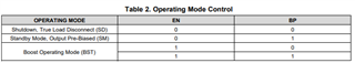
We are using this step-up dc-dc converter in the USB outputs of a device, with 3.3-4.2 V input and 5 V output. We have noticed that the BP bypass pin works contrary to what stated in the TPS61256 datasheet, i.e .:
- EN low, BP high: 0V output
- EN low, BP low: output in bypass
- EN high, any BP: power supply on, 5V output.
Looking online, I saw later that there is also a datasheet referring to the "C" model, the TPS61256C, which is actually what we are using, and in that the ball BP is renamed GND!
Now I ask you, since I need the bypass function, and also need to disconnect voltage at the outputs, can I drive BP pin high and low to turn it off and put it in bypass? I ask you this because from what I have tested it works. Or are there any contraindications / defects that I don't know that could give me problems in the future?
Thank you