This thread has been locked.

If you have a related question, please click the "Ask a related question" button in the top right corner. The newly created question will be automatically linked to this question.

BQ76940: The output of the chip REGOUT 3.3V is only about 2V.

Part Number: BQ76940

This is our circuit

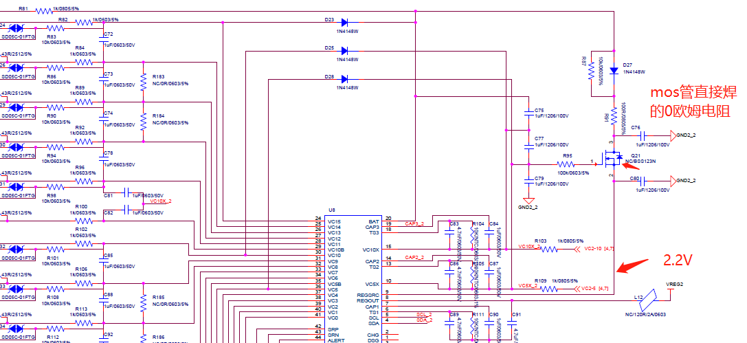
The two soldered to 0 ohms can output 3.3V, but the chip will burn, and the 3.3V output voltage will also decrease.

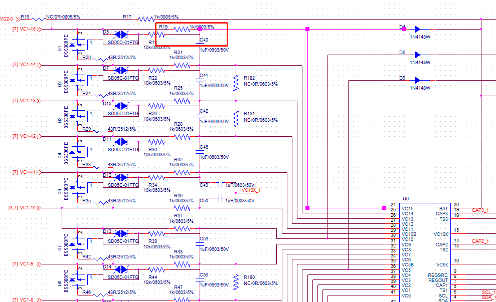
The voltage drop of the highest string of batteries after passing R19 is 1.2V. What is the reason
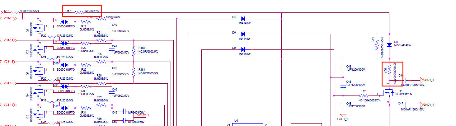
  • Hello Depeng,

    I recommend you read and follow Section 9 REGSRC Supply of the bq769x0 Family Top 10 Design Considerations application report.

    R81/R17 are unnecessary, remove them or replace with 0-Ohm.

    D4/D24 should not be connected to the REGSRC FET drain path, these should only connect to the BAT pin.

    R23/R87 are usually 100-kOhm.

    It seems you are stacking, so I'd recommend you place the diode/resistor pair in the source side of the FET. It would keep the voltage at the REGSRC pin lower and the IC would dissipate lower power. This is mentioned in Section 9 of the application report mentioned above. At lower cell voltages, your current set-up may be better. You should also be placing the drain resistor before the diode/resistor pair as shown in Figure 14 of the previous app report.

    I would also recommend you look at the schematic for TIDA-01093 and look at the datasheet schematic examples.

    Best Regards,

    Luis Hernandez Salomon