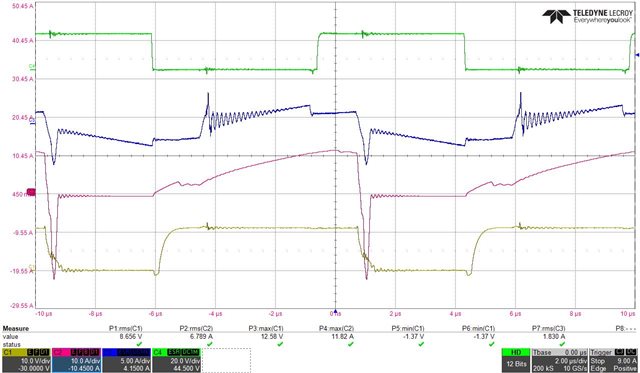
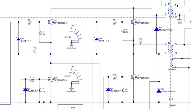
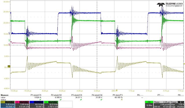
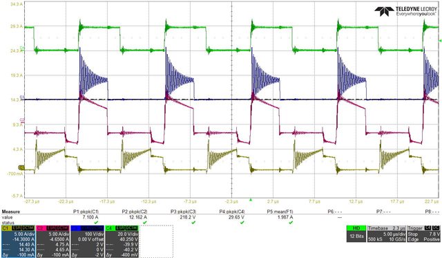
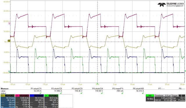
Currently the output is using Current doubler with 28951 controller ,SR control to burn SR MOSFETs as soon as they are turned on.
I'd like to ask if you can help me with the confirmation.

-
Ask a related question
What is a related question?A related question is a question created from another question. When the related question is created, it will be automatically linked to the original question.