This thread has been locked.

If you have a related question, please click the "Ask a related question" button in the top right corner. The newly created question will be automatically linked to this question.

TPS65251-2: Synchronous buck regulators are topologically capable of reverse power flow. However TPS65251 the refuses to dump excess output capacitor charge back to its input

Part Number: TPS65251-2
Other Parts Discussed in Thread: TPS65252

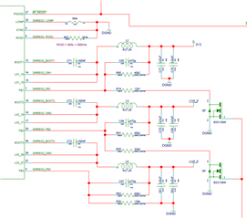
We have an application where we generate supply voltages for a Spartan 7 FPGA.  This part has some awkward power-on and most especially power-off requirements.

To fulfil the power-off requirements we arrange for the feedback dividers on the 3V3 and 1V8 rails to change to request 0.8V in each case at power-down.

What we expect to see is the charge in the output capacitors flowing back to the supply rail (12V) however and for the 3V3 and 1V8 rails to be brought down to 0.8V very rapidly.

What we see is the 3V3 and 1V8 rails drifting down to 0.8V as if they had been disabled.  This is definitely not what is required!

Why do we see this behaviour and what can be done about it?

Please note

  • LOW_P is pulled low
  • The circuit works with just fine with Richtek's RT7273
  • Hi Can you share your sch for review? and if you have power down timing requirement diagram, please share as well, which is helpful to review your question.

    BTW, what's the purpose to make "What we expect to see is the charge in the output capacitors flowing back to the supply rail (12V) "

  • There's no diagram but here the requirements:-

    From https://www.xilinx.com/support/documentation/data_sheets/ds189-spartan-7-data-sheet.pdf

    The recommended power-on sequence is VCCINT, VCCBRAM, VCCAUX, and VCCO to achieve minimum current draw and ensure that the I/Os are 3-stated at power-on. The recommended power-off sequence is the reverse of the power-on sequence. If VCCINT and VCCBRAM have the same recommended voltage levels then both can be powered by the same supply and ramped simultaneously. If VCCAUX and VCCO have the same recommended voltage levels then both can be powered by the same supply and ramped simultaneously.

    For VCCO voltages of 3.3V in HR I/O banks and configuration bank 0 the following conditions apply.

    • The voltage difference between VCCO and VCCAUX must not exceed 2.625V for longer than TVCCO2VCCAUX for each power-on/off cycle to maintain device reliability levels.
    • The TVCCO2VCCAUX time can be allocated in any percentage between the power-on and power-off ramps.

    There is no recommended sequence for supplies not discussed in this section.”

    In my application

    • VCCINT=VCCBRAM=1V, VCCAUX=1V8 and VCCO=3V3
    • TVCCO2VCCAUX=300ms
    • ramp times are 200us-50ms

    The important thing to note is that at turn off it is the 3V3 rail that must that fall first and 1V0 that must fall last.

    Regarding your comment BTW, what's the purpose to make "What we expect to see is the charge in the output capacitors flowing back to the supply rail (12V) ".  To reduce a power rail at turn off you can either:-

    (1) Turn off that channel of the supply and allow the rail to decline passively.  However the problem with this is that the load will be low because the system is in reset at this time, therefore the decline of the rail is slow.

    (2) Cause that channel to actively regulate to a lower voltage, such as 0.8V.  This will be fast, regardless of the loading on the rail.  It is an intrinsic property of synchronous buck regulators that power flow is bi-directional (and that the inductor current can be positive, negative or both within a cycle); when lowering the target voltage the charge on the output capacitor will be returned to the input.

    I do not wish to share the schematic at this time.

  • Hi Robert!

    It suggest you to provide a simple circuit of the 3.3VCCO and the 1.8VCCAUX. Just a structure, don't need specific value of component.

    Dose the target voltage in your sentence means the output of a buck converter?

    Best regards

    BSR-MV

    Shuai

  • "Target voltage" means desired output level of the buck converter.

  • Hi, Robert

    1. Could you share some test waveforms? 

    2. Maybe you can set LOW_P to high, then test again. 

  • I won't send waveforms.  However I think the problem is related to the over-voltage protection feature.

  • You think IC triggered OVP? why? 

  • Consider the 3V3 output.  A resistor divider causes 800mV to be presented to the feedback input.

    At shut down, the resistor divider is changed and then 3V3 is presented to the feedback input.  That is why I think that the OVP feature is being activated.

    However this doesn't quite explain what I see because the OVP feature is claimed to turned off the high-side MOSFET, whereas the parasitic diode should still allow reverse power flow.

  • I got you. 

    Could you measure some waveform for analysis? Probe Vout, LX, Vin in one waveform. 

  • I have given up on getting useful answers regarding my questions on the TPS65252.

    I will solve the problem by other means.