This thread has been locked.

If you have a related question, please click the "Ask a related question" button in the top right corner. The newly created question will be automatically linked to this question.

BQ76952: IC is being Over heated and Not working when separated from MCU

Part Number: BQ76952
Other Parts Discussed in Thread: LM5017,

Hi,

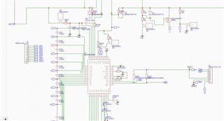
I am using bq76952pfbr. I designed a Separate PCB for BMS IC and MCU with LM5017 so that I can put MCU (Bluetooth) in a non-shielded area for better signal strength. Initially, everything works well, I can receive all data from MCU but when I remove MCU from BMS IC and try to connect again, i2c communication is not established. Then when I check IC with a thermal camera, yes IC is getting hot. Following are my clarifications.

1. I set the number of cells to be balanced to only 1 ( I don't think Cell balancing is  increasing its temperature )

2. Only when I separate the MCU board from IC, I can see failure else I have prototypes that are still working for months

3. Each and every time I Connect the MCU board to the BMS IC board I can see sparks on B+, I feel this is to charge capacitors on MCU Board

I guess fluctuations on the BAT pin is the root cause for the Issue. But I have no idea. 

  • Hi,

    Unfortunately our team is on vacation this week for christmas and new year. We will respond to you by the week of Jan 6, 2022

  • Hi Mounish,

    That seems odd to have the temperature increase without the MCU.  An increase in temperature is likely due to some increase in current into the IC.  Some suggestions:

    • Check for increase in supply current of the BQ76952 looking at the voltage across RBAT when the MCU is removed
    • Check for increase in cell input currents.  The cell input resistors are not shown on the schematic clip.
    • Check for voltage change on the signals to the board.  With the HDR attachment of H1 to H3 the MCU would seem to provide a high voltage limit on the I2C lines.  The pull ups appear provided from VCC5.  Check what happens to the SCL, SDA voltage with the MCU removed.
    • Check the voltage on REG18 (CREG18) with the MCU removed, be sure it does not rise to a higher value from the VCC5 or other change.
    • Check for change in operating mode of the FETs on the disconnection from broken GND or power or change in configuration.  I don't recognize a potential in the schematic clips, but check since the heating behavior is unexpected.
  • Hello, I cross verified everything,

    I even checked voltage spikes on the BAT pin using an oscilloscope. I as unable to figure out the problem, Please find the attachment of my schematic and let me know if there is any mistake Schematic_Smart BMS 16S and MCU_2022-01-10.pdf

  • Hi Mounish,

    In the PDF attachment I don't recognize how B- connects to VSS.  The BQ76952 VC0 has a limited voltage range compared to the other inputs.  A common recommendation is to connect the tap for VC0 to the B- on the PCB.  If the JST17 signal were connected to the wrong voltage during positioning of H2 a high voltage might be placed on VC0.  Some designs which use a separate connection for the VC0 reference point (JST17) will limit the VC0 voltage with diodes, but depending on what voltage the pin contacts that can give momentary large current through RIN17.  This does not seem to be your issue however.

    The diode D4 would seem reversed.  Normally it is desired for the R3 to be in parallel with RDSG when the DSG pin pulls low.  Again this does not seem to be your issue with the part heating.

    Z4 through Z7 are 16V Zeners, the maximum voltage allowed on SCL, SDA is 6V. So the Zeners could allow a damaging voltage on the SCL, SDA pins. If the MCU board has been off for a long time its voltages will all be at the same potential.  Depending on how pins of H1 mate, that same potential could apply B+ to the VCC5, A4, and A5 possibly damaging the BQ76952. The spark you mention indicates the circuit is able to hold the pins together with some intensity,  likely due to the capacitors, a similar current may be going into SDA, SCL before the spark of B+ and VSS.  Perhaps you could explore connecting VSS to the MCU board before mating the header.  Some designs have connectors with longer GND pins so they mate first, but even if that works you might be sure the Zeners limit the IC pin voltages within the allowed range.  Remember Zeners still have a slope, so they may have a voltage above their Zener test voltage with a high current surge such as charging the capacitors.

  • Hi,

    As you said "If the MCU board has been off for a long time its voltages will all be at the same potential.  Depending on how pins of H1 mate, that same potential could apply B+ to the VCC5, A4, and A5 possibly damaging the BQ76952" 

    1.H1 connectors are JST type and they cannot be connected in the wrong direction.

    2. I am using a 3.3V MCU and 2k pull up resistor, so when the MCU is off for a long time are you saying that they can go up to B+ voltage..? or let us say that voltage on SCL and SDA pins is 3.3V when MCU is removed suddenly, Longer exposure to this voltage is causing the failure..?, If yes what is the solution..?

    3. Actually when I connect MCU and use the bq76952 device, I don't have any problem but all of a sudden If I remove MCU with J3 and H2 connectors still connected to the board is causing the failure or when I connect MCU to the board is causing failure. Is it ok to remove MCU like this..?

    4. Does placing MCU and bq76952 on the same PCB will solve the issue..?

  • Hi Mounish,

    1. That is good to know.  Unless they are specially designed most connectors have pins with similar length but some tolerance and some play or flexibility to mate and provide contact pressure with their mating contacts.  When you bring the connectors together it is difficult to know what sequence the pins will mate.  You might get pins 1, 2, 3, 4 etc, or you might get 1, 4, 5, 2, etc or any other combination.  You may be able to get connectors specially made with longer contacts on some pins so that if those are used for ground the circuit reference would connect first.

    2. Not specifically that the board pins can all go up to B+, but rather that they all go to the same voltage.  When B+ is disconnected the converter likely discharges the input capacitor to maintain the 3.3V.  The MCU and other circuitry continue to consume current from 3.3V, as the converter can no longer provide current the circuitry (converter, MCU, & other) discharges all the capacitors to 0V with respect to its reference, or to the same potential with respect to some other reference.  When you connect a discharged board to the powered base board it is rather like connecting a shorting bar.  Not knowing which pins connect first: 

    If GND connects first the next connection will see the GND value, that should be fine for the comm signals, when B+ connects there may be a spark as the capacitors charge.

    If B+ connects first the next connection will see the B+ value, if that next connection is a comm signal the IC on the powered base board may see too much voltage, and current may flow out of the MCU comm pins starting to charge the MCU-board capacitors.  When GND connects there may again be a spark as the capacitors charge.  

    So connecting would seem to be a risk for both circuit boards. 

    3. If the issue occurs only on disconnect the description in 2 would not seem to be the problem.  Ideally if all connections break at the same time on disconnection the same potential should exist on both sides of each connector and there should be no disruptive voltages or currents.  Again with connector pin tolerances:

    If GND opens first the converter will try to maintain its output voltage by depleting the input capacitor, GND of the MCU board and all attached signals will tend to move up toward the B+ voltage. The resulting higher voltage may damage comm signals.

    If B+ opens first the converter will not have power and all signals should collapse to the GND (reference) potential. It should be like turning off the power.

    Hot plugging circuit boards in systems often takes special design for either electrical sequencing or physical sequencing of the connections. Unless you have done such design and tested for its survival I would not recommend removing the MCU as you describe.  Again you might test by connecting a GND wire between the boards to see if they can then be mated and un-mated without problems. You might also reduce the clamp on the comm lines to a value between the normal operating voltage and the abs max.

    4. Placing the MCU and BQ76952 should solve the issue as many systems have both parts on the same board and this is not a common question.  Your comment that " I have prototypes that are still working for months" without unmating the boards should show the issue is not with the circuit design but something with the disconnection or connection of the live boards.  However if you move the MCU and still have mating boards be sure the same issue does not move to another interface.  For example if the power converter is on a pluggable board and provides 3.3V, be sure mating/unmating does not put B+ on the 3.3V momentarily.