This thread has been locked.

If you have a related question, please click the "Ask a related question" button in the top right corner. The newly created question will be automatically linked to this question.

TPS61178: High current at no load

Part Number: TPS61178

Hi Team,

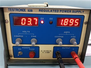
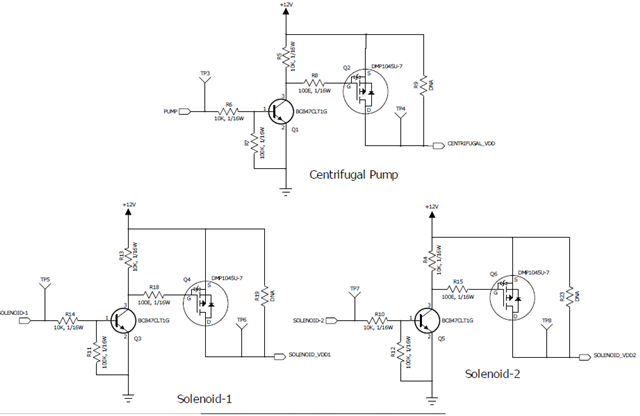
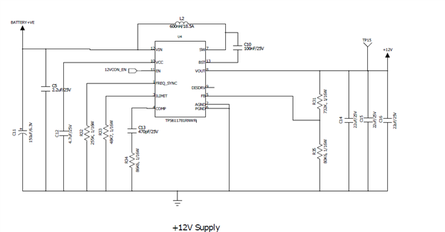
Our customer is using TPS611781RNWR in their application and noticed about 215mA no load current. I understand that the no load current is less than 1mA while the IC is enabled. What could be the cause of high current at no load?

Regards,

Danilo

  • Hi Danilo,

    Please note that customer is using the TPS611781, which a forced PWM mode device. At no load current condition, the device keeps switching and consumes some current as the MOSFET switching loss, conduction loss, inductor AC & DC loss exist. 

    But if customer sees 215mA at no load, it's little bit large. Could you let customer provides some other test result, like Iout=0.5A, 1A condition efficiency? Does customer see any unstable behaviors?

  • Hi Zack,

    I just received this feedback from our customer,

    As per your suggestion we have tested by applying 0.5Amp and 1.0Amp load at TPS611781RNWR. 
    It is observed that :
    1. The 215mAmp current is added with the load current (Total current is 720mA and 1.22A).
    2. Inductor and IC are got heated without load condition as well.
    Can you check the schematic is ok or not? If any changes needed, please let me know.
    Regards,
    Danilo
  • Hi Danilo,

    It doesn't make sense that when load current is 0.5A, the input current is 0.72A.

    To further find the root cause, please help provide below items:

    1. Vin range of this application, max Iout of this application.

    2. Full schematic, BOM and layout file.

    3. Please ask customer to provide the SW, Vout, Vin, inductor current waveform at no load, 0.5A, 1A current condition.

  • Hi Zack,

    Thank you for your response. We just received this feedback from our customer,

    Please find require details and attached data:
    1. Vin range of the application is 3.0V to 4.35V (LiPo battery)
    2. Maximum Iout will be 1.4A
    3. Schematic Design with Part Number Details
    4. Waveform at SW pin, Vin, Vout for No Load 
    5. Waveform at SW pin, Vin, Vout for 0.5A Load (0.48A)
    It is observed that 1.895Amp current drawn by device when 0.5A load is applied (See image 488mA_Load current on power supply). Hence 1A load is not applied on device.
    We have also tried to take reading for Inductor current, but it increases the input current of device hence not taken it.
    Regards,
    Danilo
  • Hi Danilo,

    Thanks for the information.

    I'll look at these schematic and let you know my feedback soon.

  • Hi Danilo,

    With same inductor value and switching frequency setting of ~700kHz, at no load condition, when Vin is 3.75V, the input current is 96mA.

    If customer didn't see obvious instability at all load range condition, it should be fine.

    The ILIM setting resistor R33 could be set to ~75kohm to set switching current limit to 10A, which is enough for this application.

  • Hi Zack,

    According to our customer,

    We have tested with changing R33 = 75Kohm. It is observed that:
    1. No load current is 165mA
    2. Inductor get heated at No Load condition

    Regards,

    Danilo

  • Hi Danilo,

    With a 900nH inductance, the inductor current ripple is little bit high. Customer could replace with a higher inductance, like 2.2uH to reduce the inductor AC loss.

    The suggestion to change R33 to 75kohm is to ensure the device switch current limit is not triggered at worst case (minimum Vin, max Iout condition)

  • Hi Zack,

    According to our customer,

    I have taken the inductor current waveform at no load condition, attached is the waveform for your reference. 
    For measurements 0.1E resistor is used in-between inductor(900nH) and SW pin. It is observed that RMS current across inductor is 4.4A.  Also observed the no load current of the Boost convert is 96mA.
    Regards,
    Danilo
  • Hi Danilo,

    Do you mean the now the boost converter input current is 96mA? It is same with our bench test result.

    Also observed the no load current of the Boost convert is 96mA.
  • Hi Zack,

    We just received this update from our customer.

    We have done run test for 15 minutes cycles of each with 0.5A load. Initially it looks stable for 12 cycles, but in cycle 13 when IC temperature rises 57 °C it stops working properly (Ambient temperature was 27°C)
    I have tested no short is observed on IC pins, and it gives output voltage equal to input supply voltage when powered it. Can you help us to understand why IC is behaving like this?

    Regards,

    Danilo
  • Hi Danilo,

    Have you checked the layout is good? Normally the IC shouldn't go to thermal shutdown with only 57C.

  • Hi Zack,

    Here are the PCB layout and schematic diagram from our customer.

    Power Board Gerber File 28022022.zip12Volt Circuit.pdf 

    Regards,

    Danilo

  • Hi Danilo,

    Not sure if I open the Gerber file correctly, I saw the AGND pin is not connected to PGND power plane on this layer. Could you help check with customer?

  • Hi Zack,

    According to our customer,

    We have checked the reply, the Gerber file send by us was wrong. Sorry for the inconvenience.
    Kindly refer the updated file and let me know your feedback.
    Regards,
    Danilo
  • Hi Danilo,

    Thanks for the update. The new Gerber file shows AGND pin is not floating and I think the layout shouldn't cause the device damage.

    We have done run test for 15 minutes cycles of each with 0.5A load. Initially it looks stable for 12 cycles, but in cycle 13 when IC temperature rises 57 °C it stops working properly (Ambient temperature was 27°C)
    I have tested no short is observed on IC pins, and it gives output voltage equal to input supply voltage when powered it. Can you help us to understand why IC is behaving like this?

    Is above failure could be replicated easily on other PCB? Did you see any abnormal waveform of steady sate at full load, no load, load transient?

    It looks the IC stops switching or some failure happened. Did you check the VCC pin voltage? Is this pin voltage incorrect?

  • Hi Zack,

    As per our customer,

    We will check steady state waveform as per suggestions and let you soon.
    The voltage at VCC pin is 3.8V when it tested which was correct.
    Regards,
    Danilo
  • Hi Zack,

    We have received this update from our customer.

    I have tested 5 PCB with 0.48A load (approximately) for 10 minutes cycles of each. I have measured Temperature of IC and Inductor(2.2uH) at every minute, temperature at IC and inductor observed stable compared to previous behavior. Following are the observations for your refence:

    Regards,

    Danilo

  • Hi Danilo,

    Thank you for sharing the test result.

    The IC and inductor temperature result at different time looks stable and good. No strange or issues.

    Is it possible that there is some soldering problem in previous PCB? 

  • Hi Zack,

    According to our customer,

    Yes that might be possible on previous PCB.
    One thing I have observed rather than this, when EN pin is disable boost converter output is 3.45V it doesn't go to 0V.
    Can you help to solve this?
    Regards,
    Danilo
  • Hi Danilo,

    It's because customer didn't add the P-channel MOSFET at output side at disconnection MOSFET.

  • Hi Zack,

    Here is the feedback of our customer,

    Thanks for the response. We have following queries:
    1. Enable/Disable is a function to start/stop functionality of IC, where load disconnection is for isolation of output load. Then how in disabled mode IC will work and gives 3.45V output? We have use external switching at the output of IC as well. Attached is the switching schematic for externally load disconnections.
    2. We observed 59mA no load current with 2.2uH inductor, can we reduce this current?

    Regards,

    Danilo

  • Hi Danilo,

    1. In shutdown mode (EN=0), the TPS611781 Vin will charge the output capacitor through Inductor, TPS611781 internal high-side MOSFET body diode. So customer sees a 3.45V Vout.

    TPS611781 has DISDRV pin for Input and Output disconnection in Shutdown mode. Customer could connect a P-channel MOSFET at TPS611781 output side and connects DISDRV pin to P-channel MOSFEET Gate. In Shutdown mode, the P-channel MOSFET VGS=0V.

    2. To reduce the current, one method is reduce the switching frequency to reduce the switching loss, inductor core loss. Another method is replacing with TPS61178, which works in PFM mode at no load and light load condition. The boost circuit power loss at no load condition is further reduced.