This thread has been locked.

If you have a related question, please click the "Ask a related question" button in the top right corner. The newly created question will be automatically linked to this question.

TPS57160-Q1: Add a beat on PH pin before bootstrap cap

Part Number: TPS57160-Q1
Other Parts Discussed in Thread: TPS54160A

Hi TI Expert

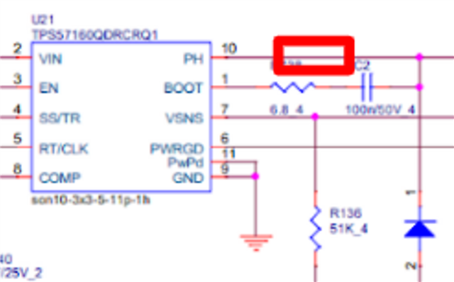
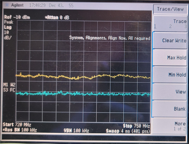
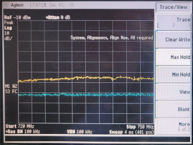
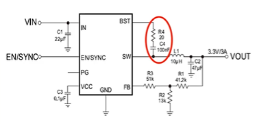
        due to RF desense issue, our customer would like add a bead on PH pin, here need TI help to check does it affect any functionality issue? what impact to add it bead on PH pin in view of TI?

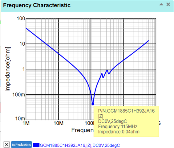
Bead PN : muRata BLM15EX331SN1.

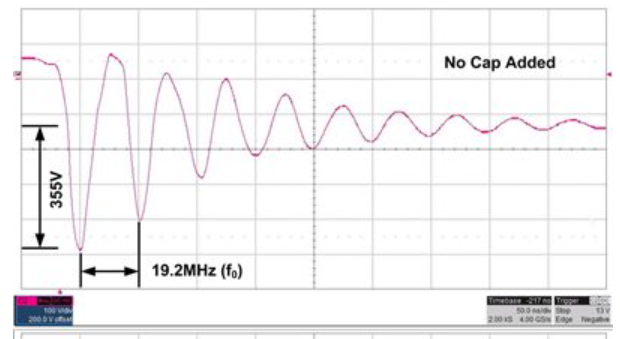
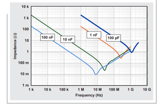
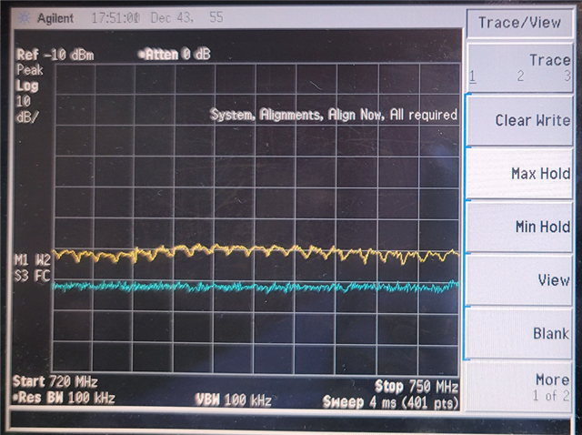
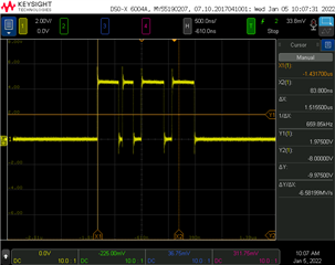
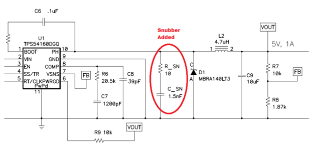
BTW, does there any other suggestion to improve the desense performance? since our customer ask why this DC converter are super-duper noisy when they use near field probe  can see the noise comes from on TPS57160Q. (LTE B12 700MHz)

  • Hi Cage,

    Before I give specific advice, I would like to see the what kind of ringing we are dealing with at the switch node. Could you check with your customer to get the measurement the ringing frequency on the switch node? Here's an example on how to do it:

    There are several general techniques that you can use to reduce EMI. If it's possible, I would strongly recommend placing the input capacitor as close to the converter as possible. Another easy technique you can use is to place a low Capacitor ESR that is notched at the problematic frequency at the input of your converter. There are other options as well, but lets see if these work. 

    Thanks,

    Andrew

  • Dear Andrew

            we will try to measure the switch node to check the ringing frequency, before it could you help to confirm can PH pin add a bead? will it make functionality or efficiency impact?

  • Dear Andrew

              Please see below screen-capture for PH pin frequency domain waveform.


              Blue color is the base line , yellow color is the broadband’s height.

            BTW, Another one chip TPS63802DLAR has same problem the screen capture as below.

    Blue color is the base line , yellow color is the broadband’s height .

    L2 Pin

    L1 Pin

  • Hi Cage,

    If you were to add a ferrite bead to the design, I would recommend putting it at the input in series with Vin. I haven't heard of anyone using a ferrite bead at the switch node (ph pin), but if the customer would like to try it out, then lets see what it does to the emissions. Of course, you are correct that there will be some conductive losses due to using a ferrite bead in series with your output current.

    By the way, could you clarify what qualifies as a failure in the frequency captures? 

    Thanks,

    Andrew

  • Hi Andrew,

    Please kindly refer to image below for ringing signal wave form. Do you have some advise?


  • Hi Nick,

    Could you try placing a bypass capacitor at Vin? This one is 3900pF ±5% and notches directly at that problematic frequency. 

    Another thing you could do is see how controlling the slew rate of the converter affects the noise. This converter doesn't have the true slew rate control features, but you can try slowing down how fast the bootstrap capacitor charges by placing a resistor in series with the bootstrap capacitor. This makes the top side fet turn on slower which increases the rise time while switching. Making the switch node signal look less like a square wave and more like a trapezoid causes harmonics to roll off faster. The tradeoff is that it increases the Trise which will increase your switching losses.

    https://training.ti.com/improving-emi-true-slew-rate-control

    Let me know if these work for you.

    Thanks,

    Andrew

  • Dear Andrew

             We had been tried the ferrite bead on input and output that doesn't work. only put it on PH pin can help, therefore we'd like to know does it make DC converter functionality abnormal? BOOT pin response delay?

           it about 10db~15db on freq captures.

  • Dear Andrew

         we have tried both solutions today, as test result there no help on LTE OTA(TIS) performance.

          do you have other advise to it? 

  • Hi Cage, could you post your schematic and layout? I would also like to know what your switching frequency is.

    Also is it possible to add a snubber circuit to the PH node?

    https://www.ti.com/lit/an/slva629a/slva629a.pdf?ts=1641489980576&ref_url=https%253A%252F%252Fwww.ti.com%252Fproduct%252FTPS57160-Q1

    Also I have no idea how the converter will function differently by adding a bead in series with the PH node. That's not a technique I have ever heard of. That's something you will have to test yourself. If it causes you to pass on EMI, then please let me know.

    Thanks,

    Andrew

  • Please give me your email address,I will send you layout and circuit for review. 

  • Thanks for the email. I am checking.

  • Dear Andrew

            I got the bead sample and tried it on EVM board, as test result the TPS54160A will be damaged no any out put then I tried it on our board, the PH pin waveform is strange and low level voltage on PH pin is -14.4V that lower than the spec as -0.6V, please help to check does PH pin adding bead may cause chip damage? 

    PH pin waveform abnormal

  • Hi Cage,

    Thank you for testing the design. It looks like the bead is affecting the loop compensation for your design, and adding some instability into your system. In the photo you sent the switching frequency isn't constant (notice how the top side fet turns off and immediately turns back on). You can confirm this by obtaining a bode plot for the PH node. As I mentioned before, putting a ferrite bead at the input would be the best way to go.

    Also, if you can, could you please place the bypass capacitor as close to the Vin pin as possible. If the return path goes through a via to ground for example, there may be some stray inductance that added into your system that is causing that noise. I cannot stress this enough.

    Thanks,

    Andrew