This thread has been locked.

If you have a related question, please click the "Ask a related question" button in the top right corner. The newly created question will be automatically linked to this question.

TPS54JA20: Buck converter shorts itself when load is applied

Part Number: TPS54JA20
Other Parts Discussed in Thread: TPS25750, ALLIGATOR

Hello everyone,

I'm building a power delivery PCB solution for a system that takes USB-C power and outputs 5V to a couple of devices.

For the USB-C PD I'm using TPS25750D and it is configured to output 15V.

For the 5V conversion I'm using a BUCK converter I found using the WEBENCH from TI. 

This is the diagram I started with https://webench.ti.com/appinfo/webench/scripts/SDP.cgi?ID=57ADCB5E2ED55CBA

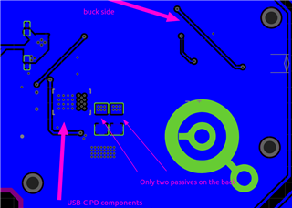
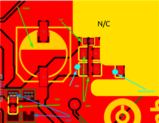
And this is my diagram. See the BUCK circuit on the right corner.

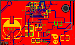
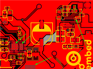
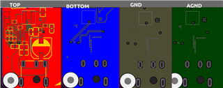
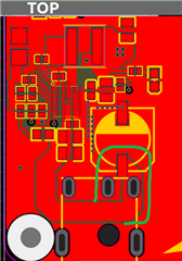
Here's the board layout for the buck converter. This is a two-layer board

With this all in mind here's what's happening:

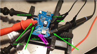
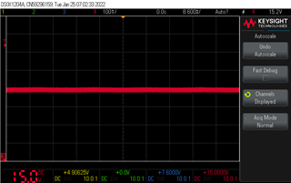
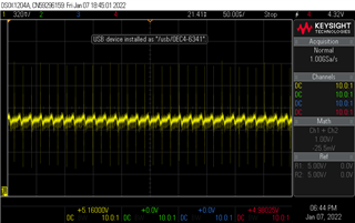
When I assemble everything correctly the SCK_L turns on and the output of the buck reads 4.93V. This means it converts 15V to ~5V. However, when I attach more load to it, it just melts down and PPHV line, GND and 5V get shorted together internally (checked for shorts on the chip itself). Note that I don't attach more load while it's on as in a hotplug and the loads that I attach are working fine otherwise (tested with a different power supply).

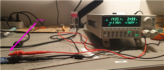
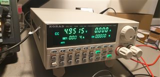
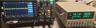
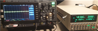
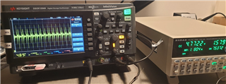
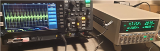
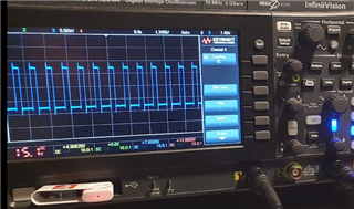
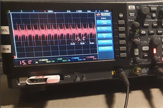
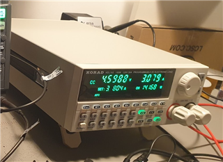
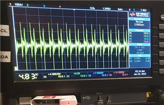
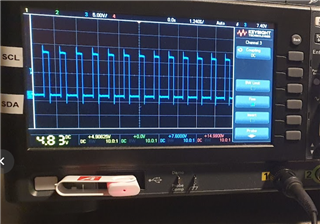
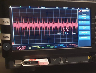
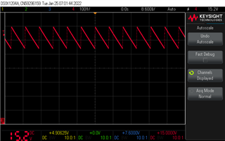
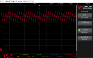
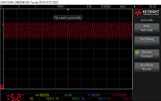
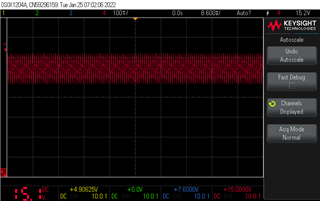
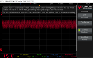
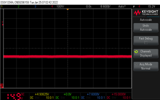
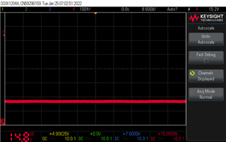
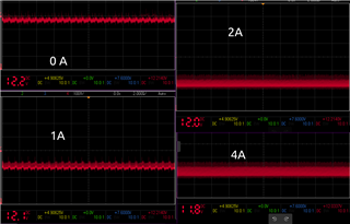
Now I did a different test using an external power supply trying to power up the buck converter (through the pads of C43 capacitor). It turns on even with loads, however, the main load which probably draws more than 1A reports risky low voltage. A multimeter will report 4.92-4.93V. Here's an oscilloscope reading:

I'm not sure what else to say. Please ask questions if something is unclear.

Many thanks,

M.

  • Hello M,

    Thank you for sharing the detailed information. I do have some follow up questions to make sure we understood correctly:

    1. What is your application requirements for the buck converter? 15Vin, 5Vout, Iout?
    2. I'm not really understanding this statement you mentioned. Are you stating that they drop to 0V?

      PPHV line, GND and 5V get shorted together internally
    3. An external power supply to TPS54JA20 causes it to behave properly regardless of the load and the concern is a low output voltage reading, correct? Here are a few speculations:
      1. Check if TPS25750D is current limited; is the device providing enough current to converter throughout all load conditions?
      2. Check that the power supply is not current limited.
      3. Where are you probing to read output voltage values? TP8?

    Thanks for your clarifications!

    Regards,
    Alejandro

  • Dear Alejandro,

    1. My requirements are 15V IN, 5V out, Typical Iout 4A, MAX Iout = 8A

    2. Actually, my concern is that the chip itself malfunctions when some more current (more than an LED being on for example / or another sink that's consuming <.2A) is drawn from it. After this, the power supply used detects a short between GND and PPHV (VIN). Later, when disassembling the chip from the PCB and measuring the pads for shorts, all GND, PPHV and 5V pads/lines have 0 OHM (shorted).

    3. The assumption is wrong, as I explain in 2), but a) is a great starting point that I haven't yet tested. I'm going to load that supply at 15V 4A (60W) to test your hypothesis. For b) I'm pretty sure it's not current limited (It's a 100W USB-C rated charger that I was able to use with different devices - some draw even more than 60W from it at 20V/5A). Regarding c), yes I tried with TP8, but also the output of the inductor/input of the capacitor on the same 5V line.

    Thank you so much for your time and consideration!

    Regards,

    M.

  • Hi M,

    Alejandro will check it and reply you early next week.

  • Hi M,

    After drawing more than ~200mA the TPS54JA20 no longer functions properly? So, a new TPS is needed to be replaced? Did I understand that correctly?

    Any updates on the test discussed on #3?

    Can you please provide the following waveforms for further inputs?

    • Capture a waveform with Vin, Vout, SW node, IOUT at no load and some load (where you start noticing a droop, ~150mA)
    • After further review of schematic, I noticed that resistor value on RMODE is below the recommended 30.1kΩ. Can replace RMODE with 30.1kΩ to set a 800kHz fsw. Also, let's increase COUT for a total of 3x 47uF. Capture waveform with updated switching frequency and output capacitance.

    Thanks,
    Alejandro

  • M,

    I would also like to mention that on the second layer (blue) the Vin capacitor is not connected properly to PGND. There is a trace that is separating the input cap from PGND. Additionally, there are no vias near pins 11 through 18 as recommended.

    Please refer to Section 10-1 in datasheet for further inputs on Layout Guidelines

    Regards,
    Alejandro

  • Dear Alejandro,

    Your input is very well received. Many thanks. 

    We will run all the tests above and return here with the results. It's going to take some time because we realized that we need to source some more equipment for this. Be right back.

    Regards,

    M

  • M, understood. We will be here to further help.

    Regards,
    Alejandro

  • Dear Alejandro,

    I'm back with some results.

    First of all, we now have a programmable load here which we used to test the USB-C PD chip. We were able to first test the USB-C PD chip. Using the TPS25750 Application Customization Tool I configured the chip to output 15V - The maximum power for this voltage seems to be 45W.

    We overloaded the chip and we were able to trigger the overcurrent protection at about 51W. Thus, we were able to draw 3A as per the application design. However, the voltage suffered a bit and fell to 14.3V. Is this to be expected?

    Here's proof:

    There was a lot of troubleshooting with the above chip and we're glad to know it now works correctly.

    Moving on to the buck converter which is the subject of this topic:

    I replaced RMODE with 30.1k Ohm, although the datasheet says you could use +/- 10%.
    I added 2x 47uF capacitors as requested.

    This is my test setup now:

    We used the same load, but this time on 5V, and ran all the tests you required for different current loads. I took a picture of the load screen which shows power, current, and measured voltage at the load. It's a matter of making sense of the numbers and understanding the behavior now. In this order I will attach captures from the oscilloscope: 5V(Yellow), SW(Blue), 15V(Red)

    NO LOAD:

    LOW LOAD (.4A): 

    After I was sure it can surpass .4A (and presumed 200mA that would break it), I really started pushing it.

    .7A


    1A:

    1.5A:

    2A:

    3A:

    When I tried to jump to 4A the buck popped at around 3.7-3.8A. As before, after failure, the GND, SW and VIN (PPHV) are shorted (0 ohm internal to the chip).

    My observations are that the noise increases in all 3 probes with the increase of drawn current. The most dramatic change happens with the 5V line which also drops in voltage considerably (4.6V at 3A). Not sure it should behave like a lipo battery Disappointed

    Those are my results. Please let me know what you think.

    One more thing. I'm afraid I didn't understand the feedback regarding a capacitor on the blue side. I might have misguided you into thinking there are more components on the backside. There are only two capacitors near the output of the USB-C PD Chip and no components related to the buck are on the back of the board. This is the back of the board without the front side SILK bleeding through. Please let me know if a misunderstanding from my image is not the case.

  • Hi M,

    Our US team will check it and reply you soon.

  • Hi M,

    Thank you for the very detailed message. Our speculation is pointing to the USB-C PD chip, TPS25750.

    The output of TPS25750 is very noisy and should not drop in voltage when supplying 3A to the buck converter. The input to the buck should stay within ~15Vin (voltage should drop at over-current limit though). Unfortunately, I am not familiar with TPS25750 device. It belongs to a different department. For the meantime, I would like to further comment:

    • make sure the output is being measured properly with correct probing techniques. Example, the tip-and-barrel technique. Improper measuring techniques can result in exaggerated output noise.
    • All outputs are VERY noisy.
    • Double-check there is sufficient output caps as recommended for TPS25750 application.

    For the layout, we just want to point out two things: (1) There are no vias for either power or ground planes. It is recommend to follow as instructed in Section 10.1 guidelines of datasheet. (2) The planes/traces for input cap C43 are not properly placed. The ground plane is very closet to the power plane pad (bottom-left of image with arrow).

    Regards,
    Alejandro

  • Dear Alejandro,

    I will try to redo the tests using tip and barrel. I have to admit that I used one of the probe's ground alligator to connect to GND and the hooks to connect to the probing points. This makes some 3 meters ground loops.

    I guess the noise should be reduced once I use tip-and-barrel but I will not assume that just yet.

    I will post my new measurements here and then further investigate the USB-C PD side.

    However, one thing here is that I learned the chip only acts as a gate that has the capacity to measure the current and voltage - So in theory the drop should be driven by the main source (USB-C wall adapter) - We can also eliminate this argument too, though, because last year I used the above layout to try to drive the buck converter using a 60W (20V) power supply that had a jack barrel-type connector. Back then I had even less experience with this system so proper testing wasn't possible but the symptoms were very similar.

    I have to say - I'm also confused when judging the choice of traces I made back then (the buck circuit wasn't a fresh design). I added the comments about the vias in the GND plane and the spacing between the input capacitor input and GND.

    I have to add one thing to the whole mix here - something we didn't discuss. 45W is not negligible power and it's wonderful it (and the double of) can be delivered through USB-C PD. However, what I forgot to mention is what copper I am using on the board. I looked at my manufacturer's spec sheet after fabrication and it looks like I used 1oz outer copper weight. I have some very thin traces in some places - for example, the SW line is .28mm wide x 2mm long and this is supposed to carry all the current from SW to the inductor. 1oz is about 1.37 mils or 0.034 mm. My calculus stops here because I'm not so sure a thin and short wire is capable to conduct tenths of watts. What is your angle with this?

    One more thing - you didn't clarify if "on the second layer (blue) the Vin capacitor is not connected properly to PGND" was a misunderstanding or I did something wrong.

    Last but not least, thank you for all of your patience and thank you for teaching me something. Your aid is invaluable.

  • Started using the tip-and-barrel measurement method as you instructed.

    The items in the yellow polygon are not connected (including buck etc) in order to eliminate causes of noise/voltage drop.

    This is the setup:

    The probe (tip and barrel) is at the cyan points (VIN/GND). The measurements:

    0 laod

    .1 A

    .2A

    .5A

    1A

    1.5A

    2A

    3A

    I also observed this "flatlining" happening after 1.5A was drawn. Not sure why it happens.

    How does the noise look now?

    I will return with some tests on the buck converter side. Unfortunately when I surpass 3.7A as said before I have to resolder new chips to the board and this takes time. Fortunately, the USB-C chip just shuts down the circuit at overcurrent.

  • Hi M,

    Our US team will check it and reply you soon.

  • M,

    PCB layout is a huge influence on performance of device. The SW line must be as
    short and wide as possible. My next steps was to get more info the traces, but you read my mind. Thank you for the details.

    Apologies -- let me clarify on my earlier comment: I didn't see any vias connecting PGND plane from Layer 1 (red) to Layer 2 (blue). It is highly recommended to have at least 6 PGND vias placed to minimize parastic impedance and lower the thermal resistance. How is Layer 1 and Layer 2 PGND connected? Also, in the previous image I attached, I circled the area in which I do not see proper layout routing techniques. The different copper planes (PGND and PPHV) are relatively close to each other. Notice
    how PGND plane is very close to bottom-right corner of C43 pad. I hope that cleared things up.

    Regards,
    Alejandro

  • I have to admit there's only one via on the buck side. On the USB-C PD it seems I respected the guidelines and I installed the vias through the large pad and later another pack of vias to the right of the chip. See attachment.

    As before, I admit the placement of the electrolytic capacitor is rather questionable -  Unless this is the cause of the misbehavior of this board, which is a prototype, I intend to find the setup which would make the prototype work and then repair the mistakes made in a future release.

    Do you think the voltage drop from the buck is what's causing the buck converter to malfunction? The drop is 0.1V at 2A which means that if 14.9V is not a low voltage, it should be possible to draw more than the 4A at 5V. But the circuit breaks at 3.8. 

    Correct me if I'm wrong but my understanding is that if I could pull 15V 3A (45W) before the buck that would mean I could output ~ 5V 9A after the buck - power losses from conversion.

    I have one more setup that I am going to test which involves a different power source through a barrel jack connector - but the buck circuit is the same except it takes 12V (so different passives to adapt to that)

  • Ok, here it goes. I have this 4 layer board on which I designed the initial circuit. I totally forgot about this board because I moved away to USB-C PD.

    For some reason, in this PCB it seems I respected design considerations outlined in the datasheet.

    I have vias, I have 2oz copper and 4 layers.

    This is the (old) pcb setup

    However old, this seems to work (somewhat?) better.

    I tested the 12V(VIN) line and 5V(VOUT) from the buck. I still have voltage drops on both.

    Although the voltage drops on the load, I observed that it didn't drop on the oscilloscope reading. You can see in the 12V video it drops down to 11.2 around max amps (the transformer is rated 12V 5A = 60W).

    Here are the measurements for the VIN (12V)


    And for VOUT (5V) on the oscilloscope, it remained relatively stable from 4.99 -> 4.96, but in the video, you can see it drops below 4V just before the chip shuts down. 

    What is very important, I think, is that the chip doesn't break in this instance. Once I unplug the barrel jack connector and wait 5 seconds I hear a thin click and when I plug it back in it works normally. I repeated this about 5 times with the same result and same values drawn as in the video where I show the power drawn from VOUT.

    I now know the copper layers/thickness and vias make a huge difference. You can see that here I also used a better placement of the electrolytic capacitor. I must have had a bad day to come with the PCB I initially presented here (the second one was made about 5 months after). However, I cannot explain the voltage drop.

    The devices that I am using cannot work with a voltage lower than 4.95. Do you know have any clue what I might do wrong?

    Later edit: I thank you for your help and patience once again. I'm studying those components and working for a startup that is ready to expand and we will use a lot of those chips in our product.

  • I've read a bit more about this. It appears that the voltage drop is normal and intrinsic to the source with load increase.

    The question is how do I prevent the voltage from falling for the devices that I'm trying to power that are fussy about voltage drops?


    UPDATE: 

    So with my old pcb everything seems to load correctly within the spec(11.5A).

    There is no voltage drop. I am just dumb and I have to review my basic electricity physics. I realized that the drop induced by the load is just affecting it's parallel line and not another device. I don't have a single device drawing more than 2-3 amps and for this I decided to add more resistance to the RFBT so that my output voltage is higher (5.2V should suffice for my device which works well in the range 4.75-5.25).

    The only left mystery now is why does the chip explodes on my main PCB, but perhaps with 0 GND vias I can't ask much. 

    I'm really surprised at how well the buck works assembled on the old PCB shown above. I was able to pull all 11.5A from it (which triggers the in/out FETs for overcurrent) correctly.

    Last thing I'm going to ask before I do a review of the board:

    Do you see anything on the PCB above from a layout point of view that needs changing?

  • Hi M,

    As mentioned previously, the board design plays a HUGE role in performance. I'm glad you were able to find the old board to do the following experiments. Feedback on board: the layout follows very similar to our guidelines. IF you will be reworking the boards, I would do a minor suggestion of making trace for Vin Capacitor a little different. Below I've attached an image showing an idea (outlined in green):

    In regards to what you stated earlier: Theoretically, you are correct. BUT, in reality -- there are other losses around the circuit. Especially with the knowledge insufficient vias, thermally, parasitic, etc. are affecting the efficiency of the device.

    Correct me if I'm wrong but my understanding is that if I could pull 15V 3A (45W) before the buck that would mean I could output ~ 5V 9A after the buck - power losses from conversion.

    Regards,
    Alejandro

  • Could you comment on this, please? Many thanks.

    AGND/GND is 0 ohm.

    The rest of the components are as spec'd. What do you think about the layout?

  • Hi, looks okay to me. Few things:
    - Make sure there are some vias connecting the power (input and GND) planes to the layers below.
    - I would also add a few more vias under the device pad VIN (pin 10, 21).
    - Make sure to trace widths are as recommend in the datasheet (Layout Guidelines)

    Regards,
    Alejandro