This thread has been locked.

If you have a related question, please click the "Ask a related question" button in the top right corner. The newly created question will be automatically linked to this question.

LMG1205: How to Eliminate Output Overshoot

Expert 1055 points
Part Number: LMG1205

HI,

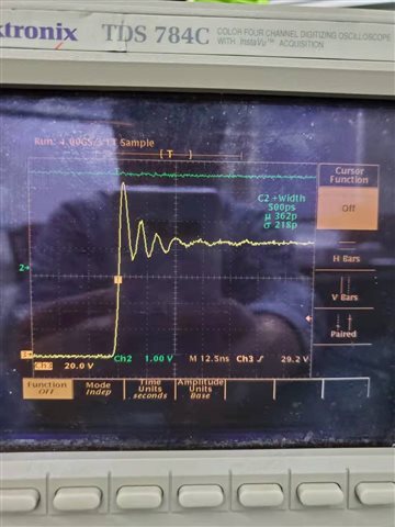
   I am currently debugging the demo board of LMG1205, please see page 5 of the attachment for the schematic diagram, LTM5113 uses LMG1205 instead. It is found that the output overshoot is very strong. When I try to increase the R19 to 10ohm, the LMG1205 is burned out. Is there any way to reduce the output overshoot? The picture is the waveform of the output terminal, at this time VIN is 80V.

EPC9087_qsg.pdf

  • Hi,

    Thank you for reaching out to E2E!

    Our expert is currently out of office, but will get back to you within the next couple days. Thank you for your patience.

    Best regards,

    Andy Robles

  • Hi,

    Thank you for your question.

    When you modified R19 to 10 ohm, did you use the same board? I'm concerned about the board being previously damaged since the voltage spike observed on the plot exceed the absolute maximum rating of the output. Also, how does the HO falling and the LO rising/falling signals look? You might also need to increase resistors R20, R23 and R24. 

    The first thing to try to slow down the signal would be increasing the gate resistor as you did. I would recommend trying this on a new board (that has not been exposed to rating beyond the abs max) and to start at lower VIN voltages (for example 15V) and then increase the voltage in small steps as you do the testing to make sure the board doesn't get damaged again. Another thing that can help slow down the switching is a capacitor from gate to source placed as close as possible to the FET pins. 

    Another factor that can cause overshoot and/or undershoot is probe GND leads inductance that add additional parasitic in the system. To mitigate this factor, I suggest using tip & barrel method measuring as close as possible to the device pins to get as clean waveforms as possible.

    Best regards,

    Leslie 

  • Hi Leslie,

    Thank you very much for your reply.

    The operation of changing the value of R19 is for the same demo board, and it worked fine before. When the MOS Driver and FET burned out, I replaced the new device and it can work normally. As you mentioned yesterday, I set R19, R20, R23, and R24 to 50ohm at the same time before the overshoot was reduced to an acceptable range. When VIN=90V, the maximum overshoot amplitude is 94V. Of course, my test method may also cause overshoot. When I increased the gate resistance to 50ohm, the FET was a little hot but not serious, and the FET was around 50°C when the driving signal was a 50KHz square wave.
    There is another question. I have observed that the frequency of the overshoot oscillation signal is about 130MHz. I am thinking if a low-pass filter is added to the Vsw end to filter out these oscillation signals, is this method feasible? Could it cause Q1 and Q2 to turn on at the same time at some point and damage the FET?

  • Hello,

    You are welcome! Another thing that can help slow down the switching is a capacitor from gate to source placed as close as possible to the FET pins. You can do this in combination with the gate resistor. Regarding the FETs turning on at the same time, the driver doesn't have a built in dead-time. I recommend to test the output signals and if you observe overlap on the HO and LO signals to program the desired deadtime on the microcontroller that's controlling the inputs.   

    Best regards,

    Leslie

  • OKay,i got it!

    Many thanks.