This thread has been locked.

If you have a related question, please click the "Ask a related question" button in the top right corner. The newly created question will be automatically linked to this question.

UCC27282: TINA simulation - lump HO waveform?

Part Number: UCC27282
Other Parts Discussed in Thread: TINA-TI

Hi Gate driver folks,

I have two questions during I simulate UCC27282 using TINA-TI. Could you help?

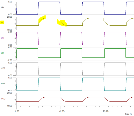
(1) For HO in simulation result, there shows a lump rising&falling edge. It looks it's because the output capacitor (C5 1.44uF) holds the VOUT voltage.

Per datasheet, the lump edges are also present in figure 35~38. Is the lump waveform from the datasheet appearing due to the same reason?

UCC27282.TSC

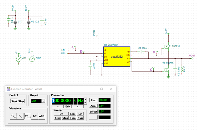
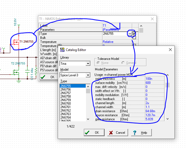
(2) Customer is using FET BSC070N10NS5 with UCC27282. To estimate rise and fall time thru tina simulation, I want to model FETs similar to  BSC070N10NS5. I believe the gate charge specification would be the most major factor for rise and fall time. Is my understanding correct?

Then could you advise how to model the transistor similar to the transistor that customer is using? Which parameter should I change?

It would be appreciated if you provide any advice as quick as possible.. Thanks!

  • Hi Ella, 

    Thank you for your questions. I'm looking into this and will get back to you between today and tomorrow. 

    Best regards,

    Leslie

  • Hi Ella,

    The initial fast rise and initial fast fall in the datasheet plots are due to the board trace inductance from the driver output to the load cap, and the trace inductance from the cap ground to the driver ground reference. These parasitic inductances appear as a high impedance at high frequency, which is why you see the voltage initially at a fast rate. Until the current develops in this parasitic inductance, the driver output is not loaded for a short time interval. 

    Regarding the transistor model, I would recommend to find a transistor that has the same characteristics as the FET that customer is using, as opposed to changing a few parameters on the model you have, since I'm not sure what the impact will be if you only change a couple of parameters. I think the best approach would be to contact the TI MOSFET group so they can recommend a TI FET that has same characteristics as the one you need. 

    Best regards,

    Leslie

  • Hi Leslie,

    Thank you for detail! But could you help me to understand which components in the figure below you're exactly referring to?

    - driver output : it must be HO or LO pin

    - load cap : maybe gate capacitance of FET?

    - cap ground : maybe source node of FET?

    - driver ground reference : it must be the node connected to VSS pin

    The initial fast rise and initial fast fall in the datasheet plots are due to the board trace inductance from the driver output to the load cap, and the trace inductance from the cap ground to the driver ground reference. These parasitic inductances appear as a high impedance at high frequency, which is why you see the voltage initially at a fast rate. Until the current develops in this parasitic inductance, the driver output is not loaded for a short time interval. 
  • Hi Ella, 

    Yes, no problem. When we test tr (rise time) parameter, we test this with a 1800pF load. The test circuit would be a 1800pF capacitor connected from the LO pin to GND. Notice that this parameter is tested with this capacitor as a representation of a typical FET capacitive load, therefore the test circuit does not include a FET, only the capacitor. Similarly, the tf (fall time) parameter is also tested with a 1800pF load capacitor from HO to HS. 

    Then, for the waveforms displayed in figures 35 to 38 in the datasheet, you'll see that the test condition at the bottom part of the figure mentions "Cload=10nF", which is considerably larger than the typical 1.8nF load. Let me re-write my message clarifying this. 

    The initial fast rise and initial fast fall in the datasheet plots for LO rise/fall time are due to the board trace inductance from the driver output to the load cap (trace inductance from LO to the 10nF cap) and the trace inductance from the cap ground to the driver ground reference (trace inductance from the 10nF cap to VSS). 

    And similarly, the initial response in the datasheet plots for HO rise/fall time are due to the board trace inductance from the driver output to the load cap (trace inductance from HO to the 10nF cap) and the trace inductance from the cap back to the driver (trace inductance from the 10nF cap to HS).

    The parasitic inductance and the load capacitor create an LC circuit, and with larger load capacitance or larger parasitics, the initial fast response will be larger, which is what you are seeing in the datasheet figures 35-38.

    Best regards,

    Leslie

  • Thank Leslie for your explanation! Clear!

  • You're welcome!