This thread has been locked.

If you have a related question, please click the "Ask a related question" button in the top right corner. The newly created question will be automatically linked to this question.

BQ76952: Abnormal SCD waveform, easy to burn out MOSFET

Part Number: BQ76952

TI experts,


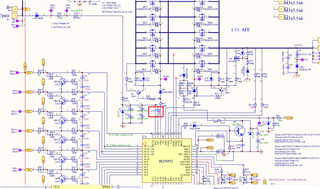
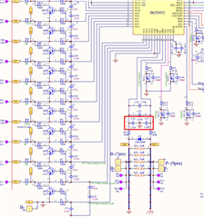
     bq76952 project, 14S6P 30Ah using LG21700M50LT cells,
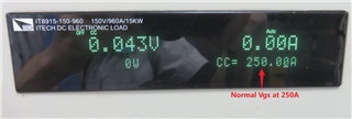
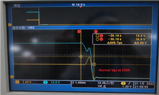
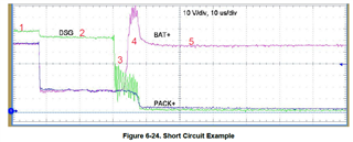
     I use the load to discharge the battery pack 250A, trigger the SCD protection, the Vgs waveform of the MOSFET looks normal.
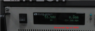
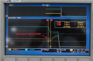
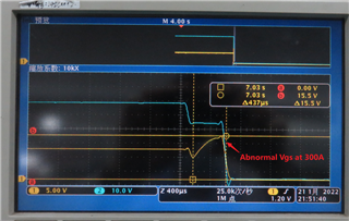
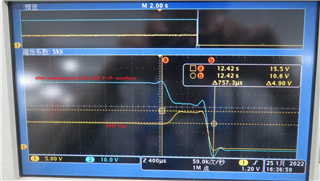
     But when we increase the current to 300A, trigger the SCD protection,      

    the Vgs waveform of the MOSFET will first drop to 7.7V, then rise to 15.5V, and finally drop to 0V. What is the reason for this? This can easily burn out the MOSFET.

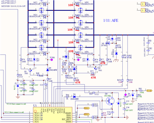
    76952-0-36-10bei-0.2mR-R00-2022-1-10(CRC).gg.csv 

      Schematic


  • TI experts,

    1. What is the withstand voltage of capacitor C23 of CP1? 14 strings of 60V batteries, can C23 use 50V capacitors?


    2. Can the CP1 capacitor be increased from 1uf/100V 0805 to 2.2uF/50V 0805?


  • TI experts,

    Will the capacitors C26+C27 of the SRN and SRP pins affect the SCD? Can these 2 capacitors be removed?


  • Hi Jmyang,

    I have not encountered the drop in Vgs during SCD although I seldom look specifically at Vgs. The circuit behavior at SCD might be described in several phases marked on this figure from the application report https://www.ti.com/lit/pdf/sluaa09 

    As an example, not matching either the example figure or your images:

    1.  Normal operation, DSG is on, charge pump is on in the high voltage mode
      1. BAT+ = PACK+ = 50V for example
      2. DSG = approx 61V
      3. Discharge FET Vgs is approximately 11V, perhaps 10V if the circuit has a diode like your D7
    2. Heavy/SCD load applied
      1. BAT+ = PACK+ = loaded cell voltage, 10V for example
      2. BAT pin of BQ76952 is held up by filter capacitor (your C19, C20), discharge to BAT+ is blocked by D1.  C23 holds up CP1 at approximately 61V
      3. DSG is driving to CP1 voltage of 61V, but current is pulled out of the pin by the DSG resistor network (your R72 etc),.  DSG current is limited to approximately 10 mA, so DSG pin voltage will drop to some level below the 61V.  In figure 6-24 above note it drops slightly, this will happen as the BAT pin filter and CP1 capacitors discharge
      4. The FET gate-source capacitance will initially pull down the gate voltage, but the current out of DSG will charge the capacitance and the voltage will rise until limited by the gate-source Zener attached (your Z10), typically 16 to 18V where it will limit.
      5. So Vgs would be expected to rise from 11V to about 18V during the SCD load
    3. The part times out the SCD delay and turns off DSG. 
      1. At turn off DSG is pulsed, pulled toward VSS until below LD.  LD should be at the PACK+ level which is the source of the discharge FET.
      2. Vgs should drop through current into the DSG pin and/or current through a turn off transistor such as your Q5
    4. The discharge FETs turn off
      1. As the discharge FETs turn off and current is reduced, the load on the cells drops and the BAT+ begins to return to normal
      2. The cells and interconnect experience an inductive response added to the unloaded cell voltage of V = L x dI/dt causing a peak in the BAT+ voltage
      3. PACK+ voltage falls to PACK- (0 V) due to the load.  If the load or short circuit is inductive PACK+ may go below PACK-
    5. The inductive transients die out, discharge FETs are off
      1. DSG is low, at or near VSS
      2. BAT+ is its normal open circuit voltage, cells may be recovering from the heavy load, 50V in example.
      3. PACK+ is low, 0 V, at PACK-

    Again I have not observed the drop in Vgs.  DSG should be higher as noted in the description.  Q5 should not be able to pull down Vgs.  One thing to look at is whether the sudden drop in PACK+ may cause a capacitor divider effect between D10 and Z9 to partially turn on M1 causing the dip in Vgs.  You might try removing R78 or R79 as a test to see if the Vgs is eliminated.  If yes there may be several ways to slow response of M1 turn on.

  • Hi Jmyang,

    1. The CP1 pin operates at 0 to 11V typical from the BAT pin.  A 25V capacitor may be suitable depending on your organization's derating rules.  A 50V capacitor seems suitable.

    2. Yes CP1 can be increased.  2.2 uF is the maximum value shown in the data sheet range for C(CP1) https://www.ti.com/document-viewer/BQ76952/datasheet/GUID-XXXXXXXX-SF0T-XXXX-XXXX-000000259873#GUID-XXXXXXXX-SF0L-XXXX-XXXX-000000259873 

    When the CP1 capacitor is increased it will take longer to reach full voltage as shown in https://www.ti.com/lit/pdf/sluaa09 section 3, but voltage will vary less when the FETs are turned on. 

  • Hi Jmyang,

    It seems the replies are grouping at the bottom of the thread rather than staying with the post where the question is asked.  I hope you can assemble with the related question.

    The capacitors C26+C27 of the SRN and SRP pins will affect the SCD response depending on the current applied.  The filter has an exponential response.  If the current is well above the threshold the delay may be a part of the time constant.  If the current is just barely above the threshold the added delay may be several time constants.

    These 2 capacitors are optional and can be removed if the transients in the system are small.  If SRP and SRN rise significantly above VSS during transient the device may reset.  See a brief description in the data sheet https://www.ti.com/document-viewer/BQ76952/datasheet/GUID-7D876EC2-60A6-42B9-9EC5-E208D1B56F00#TITLE-SLUSE13SLUSAS39258 

  • Hi  WM5295,

         After I removed the R78, the DFET's Vgs didn't have a falling waveform anymore.


    =========================================================

    =========================================================

        In the new circuit, do you think I can adjust it according to the red words below, is it feasible?


  • Hi  WM5295,

        The Vgs voltage of the DFET is too high, reaching 19.7V, as we know, the Vgs of the DFET is up to 20V, which is easy to damage the DFET, right?
    How can I lower the Vgs voltage of the DFET?

        My circuit is below, waiting for your comments.


  • Hi  WM5295,

      Can the 18V Zener be changed to a 15V Zener in order to reduce the Vgs voltage?

      The Vgs of the DFET suddenly rises during the SCD, because the voltage of P+ (that is, the voltage of the S pole of the DFET) drops at this time, while the voltage of the DSG remains unchanged at this time, so the Vgs of the DFET becomes larger? Is my understanding correct?


  • Hi Jmyang,

    Since removing R78 eliminated the dip it is apparently the clamp turning on unexpectedly causing the dip.

    In the new circuit C104 will resist movement of the M1 gate when Pack+ changes suddenly.  C104 should be "much" larger than the D10 capacitance.  Large resistors like the 10M R80 would make the clamp turn on and off slowly.  There are a few considerations for the clamp with reverse voltage:

    • When PACK+ starts to go negative you want the clamp transistor to turn on in time to prevent discharge current from the main path.  So your voltage divider of R79 and R80 will normally put most of the reverse voltage across the gate-source of M1, or R80 is typically large and R79 rather small (see the EVM).  You likely don't want a situation where if the user applies something like -12V and the M1 does not work and the battery continues to discharge.
    • When the pack has a reversed charger attached you want the clamp to hold the gate-source voltage of the power FET below its Vgsth level.  So if your normal charge voltage is 60V and the user somehow connects that in reverse, there will be a voltage divider from the DSG pin at 0V to the PACK+ at -60V.  In your circuit that will be through R72, D7, R78, and M1.  Since M1 is on and ignoring D7, it will be basically between R72 and R78, so you want R78 small (the EVM did not have a resistor) and R72 (the EVM had about 10k).  I know you are adjusting values, but these both show 100 ohms at present  That would give about -30V on the gate, so the power FET would come on and not allow the PACK+ to reach the -60V level.
    • Consider the power dissipation of the resistors in the reverse voltage scenario.
      • For R72 (with small R78 so the power FET turns off), most of the negative voltage goes across this resistor so it must be sized for the power.  For the EVM a large value was used, and a diode was used so the effective turn off resistance was smaller.  When driving a lot of FETs turn on does slow due to that larger resistance, consider a circuit similar to figure 6-21 in https://www.ti.com/lit/pdf/sluaa09 if you need the low resistance for faster turn on.
      • For R79, it will have about the reverse charger voltage minus the Z9 voltage minus the D10 forward voltage.  The power comes from the reverse charger, but consider the resistor rating and the heat in the battery.
    • DSG on the BQ76952 is not intended to and will not go very negative. If much current is pulled from it it can violate abs max.  If there is much current pulled from the net consider the D10 Schottky shown in the EVM.  Consider similar diodes for LD and PACK pins.  These were not populated on the EVM. 
    • If the pack inductance is large for a short circuit like event PACK+ can go below PACK- in transient and the clamp circuit can come on.  In this case you may want a resistance like R78 with a similar value to R77 to avoid a very fast turn off and resulting cell inductive voltage response.  Just remember the R78 value must be balanced against the R72 value as noted above.

    Yes 19.7 V seems uncomfortably close to the 20V abs max of the power FET Vgs.  You might check the scope sampling and settings to be sure the value is real. Check the Z10 location and trace widths on the layout to be sure they can limit the voltage effectively.  Check the test current for the Zener voltage, the voltage above the Zener value would indicate more current than the test value.   The DSG pin can only sustain about 10 mA from the pin, transient current could be higher. 

    • "Can the 18V Zener be changed to a 15V Zener in order to reduce the Vgs voltage?"  Yes.  Remember a Zener has a leakage current typically at about 70% of the Zener voltage, you don't want it loading the charge pump excessively at normal voltage. 
    • Larger R72 could also reduce the transient current in Z10 and the resulting voltage.  Recall the note above that this resistance needed to be large on the EVM for the reverse voltage situation.
    The Vgs of the DFET suddenly rises during the SCD, because the voltage of P+ (that is, the voltage of the S pole of the DFET) drops at this time, while the voltage of the DSG remains unchanged at this time, so the Vgs of the DFET becomes larger? Is my understanding correct?

    Yes, correct.

  • Hi  WM5295,

         After replacing the 15V Zener tube, the waveform seems to be normal.