This thread has been locked.

If you have a related question, please click the "Ask a related question" button in the top right corner. The newly created question will be automatically linked to this question.

TPS735: Regulated 3v3 output is 2v97 into 4K8Ω 3v3 rail bus.

Guru 55913 points
Part Number: TPS735
Other Parts Discussed in Thread: LM94022, INA240, , TPS737

Hello forum,

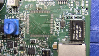
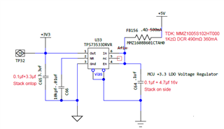
I have system with 2x 73533 LDO regulator input +5v04. One LDO has +3v307 isolated output to feed several discrete TI devices. The other supply MCU (105°C temp range) VDD rail is +2v97 minimum thus has terrible EMI rejection, easily crashes MCU.

Replacing the LDO (+2v97) made no difference, output into unpowered 4k8Ω rail load, LDO barely gets warm not hot. Oddly same PCB layout for different TI MCU (same class 85°C) maintains +3v309 into unpowered 4K3Ω VDD rail load. Both PCB has same +5v04 150MHz bucking regulator via 1KzΩ, 490mΩ DCR 350mA ferrite with 4.7uf+100nF(parallel) at the input pin 6. Reducing the ferrite impedance made no difference to LDO output (2v970) hence the higher 1kzΩ now remains. The LDO digital ground pin plane is some-what isolated from larger buck regulator analog ground plane via FB1 (0Ω <50mohm) resistor to further reduce EMI on +3v3 rail feed to MCU.

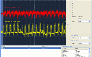
Yet the higher temperature MCU class (105°C) VDD rail (4K8Ω) appears to pull LDO output down to +2v97 causing terrible PSRR and poor rejection of EMI. The LDO output has 3.3µF+100nF (parallel) - even replaced with 4.7µF made no difference, output remains +2v97 in the EMI danger zone of the MCU.

What to look for cause of LDO with +2v97 output anomaly?   

  • Hi GI,

    Can you please share a snippet of the LDO schematic? This is pretty far outside of the DC output accuracy over operating conditions spec of +/-2% so it is hard to say without seeing how it is configured.

    Regards,

    Nick

  • Hi Nic,

    I changed the MCU to low temp version (85°C) yesterday, but the same output (+2.97) remains even with replacement LDO regulator. Also changed +5v buck regulator and checked circuit passives, +5v rail remains +5.01v into both MCU LDO's pins 4 & 6. The low temp MCU rail was then 4k6Ω same as the PCB described below. With MCU remove the 3v3 rail was 8K7Ω if that is any help.

    The +5.01 is the same input level on both PCB's LDO regulators. The main difference between the two PCB's being MCU +3v307v LDO regulator was hard soldered to PCB with Pb free rosin core (SnAgCu 280-300°C) and the +2.97v PCB used Pb free Chipquick SnAuCu low temp (235°C) solder paste for regulator passives too. The solder paste is bright shinny (U33) ball contact to LDO side pins no issue of DG pin 3 contact. FB1 (0R <50mΩ) separates AGND from SGND plane both top and bottom PCB islands. SGND is much quieter than AGND with 3x buck regulators and higher voltage switching devices. 

    Oddly full solder paste PCB secondary LDO regulator and rosin core LDO both have +3v310 output rail for 3x INA240 and 2x LM94022 temperature sensors. It seems the LDO output (MCU rail) drops with minimal current demand (idle) on the ferrite chip feeding pins 4 & 6. Ended with 1kzΩ, (DCR 490mΩ) after replacing 600zΩ (DCR 420mΩ) 600ma ferrite chip on bottom of PCB trying to figure why the MCU was faulting into latch up condition with slightest transient on +3v3 rail. 

    Solder paste PCB top U33 (TPS735) for MCU VDD rail. Notice solder ball (VIA) next to pin 4 (U33) is visible bottom side VIA too.


  • Hi GI,

    Have you reworked the LDO at all since it was reflowed? In the image it looks like there is a lot of solder on the pins, and I wonder if there is leakage from OUT (pin 1) to NR (pin 2) that may be offsetting the internal voltage reference and causing the anomaly. 

    Regards,

    Nick

  • Hi Nick,

    Have you reworked the LDO at all since it was reflowed?

    Twice LDO was removed for inspection (10x magnification) and replacement old picture, since removed large solder ball/s. The 10nf NR cap was removed for 100nf and back to 10nf not in contact with pin 1 to 2. Also cleaned LDO area with flux off first burnished solder mask between pins 1 & 2 via end of toothpick to remove hard solder paste residue.

    How-ever the hard soldered LDO does not have the thermal pad in direct contact with copper plate or two thermal transfer vias under it. Oddly the reflow LDO measures +3v307 from AGND to Pin 1 yet DGND pin 3 is the output reference ground. The thermal pad measures no resistance to pin 3 up to 30MegΩ via DMM but suspect thermal pad actually has a higher impedance of internal contact. 

    I was past informed the thermal pad had no internal connection to pin 3 but that is the only thing mostly differs between the PCB's under test.  

  • Hi GI,

    I'm not seeing a good reason for the inaccurate output voltage. It is weird that the reflow LDO output is correct relative to AGND but not DGND. With an isolation resistor of <50mΩ and 65uA max GND pin current there should be very little difference. 

    Is there any more of your schematic that you could share that shows how the LDO is connected to the MCU?

    Thanks,

    Nick

  • Hi Nick,

    Saturday I pulled FB156 out both PCB to check input supply currents. Oddly they are both cycling current even with FB1 (ferrite <20mΩ or R0<50mΩ) on +2v972 to 2v976 PCB, current cycles 138mA to 144mA. The other PCB +3v307 with FB1 (R0<50mΩ) current cycles 119mA to 122mA little to no heat output. Neither LDO should be cycling current with so little current demand or Tenma 6000 count DMM is giving odd readings.

    The higher current LDO top of case cycles hot (50°c) to then cooler cycles after some run time. That LDO has solder paste thermal pad contact with top layer foil (solder mask) under LDO are 2 exposed via annulets leading down to large under side foil region. Upon removing the LDO there is distinct solder paste flow contact visible top of via's. For some reason the foil directly under LDO had resist mask with only larger annulets exposed. Same solder mask for secondary LDO same PCB, has +3v309 output but much lower load, idles in microamp region.       

  • Hi GI,

    Looking at the layout, it looks to me like U33 pin 3 is connected to AGND, but you mentioned above that pin 3 is connected to DGND. Were you talking about a different IC than U33? Or do you mean that is because the input to U33 is the output of a buck regulator which is referenced to DGND?

    Have you observed the input and output voltages on an oscilloscope? I wonder what the voltages look like since the load current seems to be shifting in some way, possibly oscillating. 

    Is the MCU the only load for U33?

    Thanks,

    Nick

  • Or do you mean that is because the input to U33 is the output of a buck regulator which is referenced to DGND?

    Hi Nick

    Anything below FB1 is DGND and above FB1 (buck regulator U10) is AGND. Pin 3 is NRc to DGND side. The secondary LDO has the same layout though pin 3 DGND originate 3" away from FB1 and regulates +3v301 into 13kΩ load. Will check if secondary LDO oscillates input current too.

    Yesterday swapped out primary LDO with secondary LDO that was +3v301 into 13kΩ load. The primary LD0 then idles bit higher (+3v298) and have noticed Pin 1 seems to quickly peak 3v301 (auto-range DMM) then idles output +3v298. Perhaps internal overshoot pull down (400Ω) is cycling? The U10 buck +5v output has 44µF ceramics to produce a softer startup with less switching noise. U10 with enable pin level set by divider R45, R46, C74 well below bucks input threshold +24v to +40V, latter during this testing. I have to make updated scope captures of U33 and U10 during idle times, below capture is outdated.


    Is the MCU the only load for U33?

    No R157 supplies CAN chip removed during testing. Also two potentiometers, between +3v3 and AGND, (100k and 20k) 20k pot with two external resistors 20k to AGND and 2k on +3v3 rail. Have removed the ferrite feeding 20k pot past testing. Non the less the LDO input current (idle) switches on both PCB's though one LDO (VDD) maintains +3v301 output with same two potentiometers

    Seemingly primary LDO overshoot pull down circuit is causing input pins 4,6 current swings, 400Ω roughly (0.0082525 Amp) on both PCB's. The DMM is slow may not detect the full 8mA swinging. Anyway that may account for the slow rise then runtime fall off of device junction temperature?

    7.3.5 Transient Response
    As with any regulator, increasing the size of the output capacitor reduces overshoot and undershoot magnitude but increases the transient response duration. In the adjustable version, adding CFF between the OUT and FB pins improves stability and transient response performance. The transient response of the TPS735 device is enhanced by an active pulldown that engages when the output overshoots by approximately 5% or more when the device is enabled. The pull-down device operates like a 400-Ω resistor to ground when enabled.

  • Hi GI,

    I tried sending you an email to the address listed here but it failed to go through. Please contact me at n-butts@ti.com. I would like to see a more complete schematic because it is difficult for me to try troubleshooting this with only the description of the connections you have provided. 

    Thanks,

    Nick

  • Hi Nick,

    Rather PM you the PDF has notes all over it also there is no TI stock TPS735 and many other LDO in the same family tree. 

    However it seems solder paste LDO the DGND and AGND is 170Ω across FB1 pads and hard solder LDO >13kΩ across FB1 pads both FB1 removed. This explains DGND isolation being lost on the solder paste LDO when it is installed. Yet the solder mask seems ok, LDO removed the 170Ω goes away.

    It seems several replacement LDO's may be producing internal resistance across DGND to AGND solder vias when installed. 

  • Hi GI,

    170Ω seems like a lot from parasitic resistance due to solder. 

    Do you want a different part recommendation then?

    Thanks,

    Nick

  • Hi Nick,

    Have two devices caused low output voltage pin 1 from resistance thermal pad to pin 3, out of circuit.  It would seem the thermal pad manifested internal issues when solder pasted to AGND. I tested both LDO for resistance pin 3 to thermal pad prior to first installation. The thermal pad solder mask has secondary annulare outside each VIA there was no contact from solder paste to any other pin.  

    Lucky to have 2x TPS735 left (used) and placed a small silicon heat pad under primary LDO to fully isolate AGND from DGND still have thermal transfer. Under the secondary LDO 200°C capton tape to isolate pin 3 from thermal pad AGND. The two replacement LDO's are both reading +3v301 pin 1 to DGND and across FB1 3v305 - 3v307. The reason to isolate both devices from perceived transients, again hard soldered devices did not have any PCB contact to thermal pad. It seemed unnecessary for 500mA device to source under 200mA need of direct thermal contact to PCB. Seems correct as the hard soldered LDO's pin 1 (+3v301) after 12 months of repeated testing with no thermal pad contact to PCB other than radiant transfer.

    Do you want a different part recommendation then?

    I don't think there is reverse current out pin 6 and overshoot protection desired due to buck regulator turn on ramp. Any suggestions such as TPS737 may help if it has overshoot protection.

    Thanks for efforts Grinning   

  • Hi Nick,

    BTW: The replacement primary LDO is staying cool now. So later removed heat transfer pad, no solder paste thermal pad to PCB radiant transfer only. The bad LDO thermal pad reads 420Ω to pin 3 on one removed (suspect the over shoot resistor). Another LDO reads 180-240Ω depending on polarity of DMM probes. The LDO's were older stock, primary LDO baked via ramp heat profile (240°C peak). Both LDO's were initially placed on stencil applied solder paste VIA's resist mask annular rings, very small dots of solder paste. 

    Regards, 

  • Hello GI,

                  Nick is out today, we will get back to you on Monday (02/07) next week. Thanks!

    Regards,

    Srikanth