This thread has been locked.

If you have a related question, please click the "Ask a related question" button in the top right corner. The newly created question will be automatically linked to this question.

TPS61178: Part not working properly

Part Number: TPS61178
Other Parts Discussed in Thread: TPS61288,

We have a design with this part that does not work. We have this design in 2 different PCBs. It is a 8,4V input and 12V 2A output. The behavior is completely different and nothing seems to make sense. Here is the schematic.
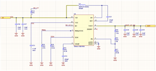
PCB NUMBER 1:

On our first prototype for the design number one the part worked properly (excepting a small issue that when the load was high enough for the part to enter PWM mode it did not return to PFM mode as the load lowered, even with no load at all, we needed to switch off the input and restart it to return to PFM). We have found problems with the second prototype of this first PCB. The part only works properly for loads below 0.4A. With higher loads the output falls to aprox. 10V. The FB signal also falls according to the output voltage The main abnormal behavior I can see is that the COMP signal also falls from more or less 1,5V to 1,2V. According to the block diagram of the datasheet COMP should increase as FB gets away from the 1.2 reference. When this happens, all the signals remain at that levels even if I lower the load, including disconnecting it. 

My questions for this PCB:

  • Why is the COMP signal falling down together with FB signal. Usually the behavior is the opposite.
  • Why does the part get stuck in PWM mode even with no load?
  • When the part gets stuck in PWM mode the signal at the SW pin is the same even with no load, but the current consumption from the input is consistent with the load applied at all times. At the SW pin we can see that the frequency of the signal is the proper one (according to Rt, 1,1MHz) and that the duty cycle is 20% aprox. Why is this signal not generating current on the coil and therefore not in the input? It is supposed that with that signal the current on the coil should raise and then be transferred to the output capacitors, but there is no current consumption at all excepting the switching losses.
  • Why is this happening and how can we solve it?

PCB NUMBER 2:

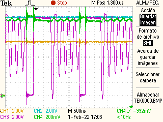
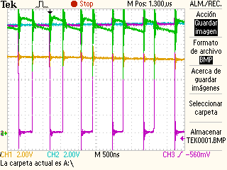
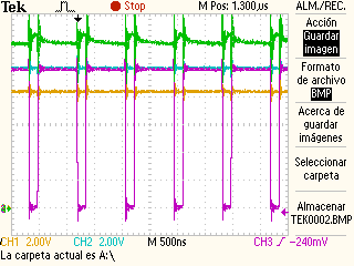
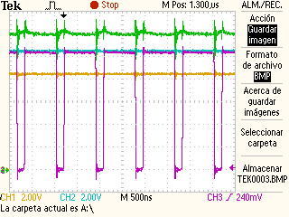
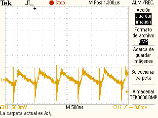
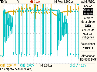
We mounted 2 different prototypes and both of them have the same behavior. We can only achieve the required output voltage if we start the converter with no load and then slighly raise the load, but we are not able to reach the 2A output. Before that all the signals that were more or less stable started to show strange waveforms. We can see ramps on FB signal, as if there was a capacitor connected there. The COMP signal falls to 0 and performs a strange recovery waveform. The SW signal shows that both FETs are off sometimes. I am attaching a couple of waveforms, one when working properly and another one when it does not work.
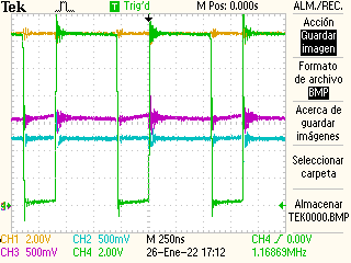
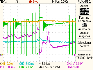
Yellow is output voltage

Green is SW pin

Blue is FB pin

Purple is COMP pin

My questions for this PCB:

  • Why can we see capacitor slopes on FB when output voltage is stable? It is supposed that FB is just a small copy of output. Is there any internal capacitor at FB pin?
  • Why that weird signal on COMP? It looks like it is not following the inverted version of FB. According to the datasheet the signal on COMP is clamped for not going too low. Why is it falling to ground?
  • Is it normal that both FETs are switched off at the same time?
  • Why is this happening and how can we solve it.

Regards.

  • Hi Carlos,

    These behavior are not expected. 1)The loop stability may be one of the reason. You can design compensation network parameters according to section 9.2.4.4.2 and test the device again. 2) Please share the layout and I check it. And provide more waveforms. 3)Please make sure the device you are testing is from ti.com or mouser.

  • Hi Xu, 

       What waveforms are you interested in? I think the ones I already provided are showing all the relevant signals for PCB number 2. As for PCB number 1 the waveforms are missing I am going to capture them and send to you. My idea is to capture the same signals unless you point out that you are interested in any other signal.

        I will also attach both layouts, for PCB number 1 it looks quite well done but for PCB number 2 the grounding is not the best one.

        Anyway, what I can tell you is that I think (not sure as I am not the designer, it was performed by someone that does not belong to the company anymore) that the whole design was made using webench, so the compensation network should be OK. However, before writing to you we have tried with many different values for the network and none of them seemed to work, we have also tried with higher coil values, but the behavior was similar in all cases.

       I can't tell you where the IC came from as I received the board assembled, I am going to try to retrieve that information. Anyway, what is driving me completely crazy are 2 issues.

    1. Why is the converter working properly sometimes? If it was damaged what we would expect is that we could never make it work,
    2. Even worse, when the converter starts working in PWM mode it never returns to PFM and it gets stuck with always the same waveform on SW pin, which is proper frequency (programmed by Rt resistor) and 20% duty cycle. Same waveform should demand same current for the input and provide same output power, but the current drawed from the input is according the load we are demanding, and with no load there is no current consumption on the input (only the switching loses). Even if the IC is damaged, how could you explain this? A coil receiving switching signal but drawing no current is against everything I know so far about power electronics... 
  • Hi Carlos,

    The reason I want to know the device come from is that I want to make sure you are using genuine.

    For your PCB1, it always works in PWM, right? You may check if TPS611781 is used because this version only works in FPWM.

    For your PCB2, the load capability is not expected as your schematic. Please check the ILIM resistor first. And please provide the waveform of VIN, Vout, SW and IL. Note that the input voltage should be measured on C26/C27 because the is voltage drop on the input trace, also measure the output voltage on C28.

  • Hi Xu,

    I am still trying to get the origin of our ICs. I will let you know as soon as I get the information.

    For PCB1 your statement is not right. I have been performing further tests on it to retrieve more information. It started working in PFM but after raising the load it started to work in PWM (as it must do). If I raise the load a little bit more then the output falls to 10V, the feedback falls to 1V and the COMP signal falls to 1,2V aprox (which according to the datasheet is the minimum voltage at that pin, but should happen when the FB is above its 1,2V reference, not when it falls). When the device enters this situation it is not able to recover itself, even if I remove the load. In that case it shows a minimum current consumption (because of the switching loses) but all the signals remain the same (output voltage, SW signal, FB and COMP). What I know now is why the converter is not showing any consumption with that SW signal. What is happening is that the current is rising in the inductor in the ON time as expected (20% duty cycle), then at the beginning of the OFF time it transfers that current to the output capacitor, but when the current gets to 0 the high side FET is not switching OFF, so the current is becoming negative on the inductor and the current is flowing back from the output capacitors to the input capacitors. At the end there is no effective current consumption because the current is continously going ahead to the output capacitors and then coming back to the input capacitors. So for this PCB1 my main concern would be to know why the COMP signal is falling to its lower value when the feedback is far below its reference, why it gets stuck at that level even if I remove the load and why the IC is not going back to PFM mode (according to the datasheet the condition to return to PFM is voltage on COMP getting lower and it is at its lowest possible point).

    For PCB2 Ilim has been checked and rechecked, and we have tried with even lower values, but the behavior does not change at all. I have not worked anymore on it so I do not have further information to give, I am focusing first on solving the issues of PCB1.

    I am going to provide the waveforms you want for both PCBs and both layouts.

    Regards

  • Hi again Xu,

    I have confirmed the origin of the ICs, they were purchased in Mouser.

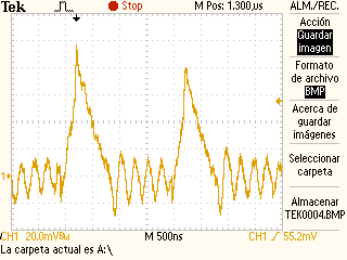
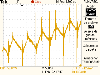
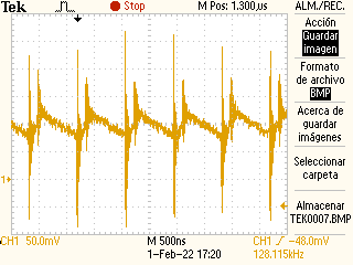
    Following you have the waveforms you asked me to capture. As we do not have a current clamp for oscilloscope I had to capture IL using a SHUNT resistor and as the GND for each channel are not isolated it was not possible for me to capture that signal at the same time, so the IL waveforms come in different images. 

    Yellow is Vin

    Blue is Vout

    Purple is SW signal

    Green is COMP signal (which is the one I always suspect is not working properly).

    First waveforms are when working properly at 12V 0,1A

    As you can see there is no negative current as the high side FET goes OFF when current gets 0

    Second group waveforms are when working properly at 12V 1,3A

    Last waveform is with a wider span so you can see how the current throught the inductor rises and after several cycles it stops switching because the output is high enough and then starts again.

    Third group waveforms are after the system malfunctions getting stuck at  aprox 10V, 1,3A

    Last group waveforms are after the system malfunctions getting stuck at  aprox 10V, lowering the load to 0,1A

    As you can see when the system starts malfunctioning it does not matter what load is connected. The input and output voltages and the SW signals are nearly the same, as is the current throught the inductor, that when the current demand is low, it becomes negative because the high side remains on.

    My main suspicion is on the COMP signal, according to the datasheet it has a span from 1,25V to 1,9V, depending on the FB signal. In all these waveforms it is based around 1,2V and with strange waveforms (I was expecting nearly a DC signal on that pin) and with FB far below its reference as the output is around 10V, COMP should sit around 1,9V, not at 1.2V Could you please explain why it is not sitting at 1.9V?

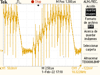
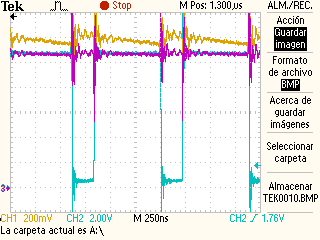
    Finally I am attaching 2 more waveforms hoping they help you to detect our problem. In the first one you can see SW and COMP with a wider span

    In this last one you can see SW, COMP and FB when malfunctioning at 10V

    Anything else you need from my side. Please do not hesitate to ask. Regards

  • Hi Carlos,

    Sorry for the delay. I just came back from holiday.

    Yes, the behavior seems strange to me too. At 12V 1,3A the inductor current should be continuous. I'm afraid if probing COMP pin will bring noise and make the device work unstable. Could you stop probing the COMP signal and capture VIN, VOUT ripple and SW waveform? Please make the horizon scale of SW large so it will not cover other waveforms. Another reason may be unstable. I used the calculation tool and the recommended Rc=15k, Cc=4.7n, Cp=56p. Please use these parameters for a try. If it does not work, please share the layout so I can check it.

  • Hi again Xu,

       Sorry for the late response, I have been busy with other issues. Following is the information I have compiled so far.

       The IC on PCB1 was damaged, after replacing it the system started to work properly for almost the whole range we needed. It looks that probing COMP was not a big issue as the behavior with the damaged part and the new one was similar when probing and when not probing. For the IC that was OK, COMP level was based around 1,5V and not 1,2V.

        However we are still experiencing a couple of issues that we were not expecting on this PCB1.

    • We are not able to reach continuous 4A at 12V, around 3,5A we start to see that the output voltage slowly rises and at 3,8A it starts to rise faster and then the part autoshutsdown because the thermal protection is triggered. We are sure it is caused by the thermal protection because we have put a fan in front of the PCB at the lowest speed and then we are able to reach 4A with no output voltage rising. We have taken measures on the input and the output power, and the power lost in the IC is about double than it was supposed to be according to webench. Could you please explain this high power dissipation? As it is not possible for us to include a fan in our design we would need another method to prevent the thermal protection to be triggered.
    • There is a second issue with the working mode. When we start at light loads the IC starts in PFM as it is supposed to do, at higher loads it works in PWM mode which is also ok. The problem is that when it works in PWM mode it never returns to PFM even if we lower the load to 0, so the efficiency is horrible. We need to switch off and then on the input to make it work again in PFM. Why is it not automaticly going back to PFM?

    Regards


  • Hi Carlos,

    1) If you need so higher output power, 680nH inductor is not suitable since the current ripple is large, you should use like 1.8uH to reduce core loss of inductor. The switching frequency should be set lower to handle the power dissipation. And the layout should be large enough for better thermal environment.

    You may redesign compensation network according to section 9.2.4.4.2 in datasheet.

    2)This issue does not make sense to me. The device may be damaged again. You can try the changes above first. 

  • Hi Carlos,

    Additionally, if you don't need load disconnection function but need higher output power, TPS61288 will be a better choice.

  • Hi Xu,

       I thought exactly the same, that the inductor was too small, and because we had here 1,8uH from other converters I did exactly what you are suggesting. It improved a little bit but we are still facing the thermal shutdown issue without reaching 4A. When I told you that the power dissipation was about double than expected, I was talking about the 1,8uH redesign for that switching frequency. We have not tried to reduce the switching frequency, we will do it and I will let you know the results. As our inductor is higher now we have margin to do that reduction. Is there any frequency value you recommend? In addition we would have a look at TPS61288. In case it is footprint compatible, it could be an option, if not I am afraid we have to go on with the current part.

    Regards.

  • Hi Carlos,

    I'd suggest trying half of the current frequency. TPS61288 does not have the same footprint but it is better for your application. Of course, you can using TPS61178 and optimize the design.