


Other Parts Discussed in Thread: LM5155, LM5156
Hi sir,
I am designing a boost converter of 48V, 3A output with a 24V input power supply. It is a nonisolated dc-dc converter.I have taken design from webench. I have designed this model two times earlier also.
But it gets fail.
In my first design, I haven't considered any design guidelines. And because of that, my module faces the EMI effect. Due to the EMI effect, I am not getting the desired output. I found that above 30mA load I get voltage drop.
so it is totally unreliable for me.
Owing to this I redesigned it by considering design guidelines. in design guidelines, they have said that the output loop should be as small as possible and the switching node should be small. I had done all these things.
and In my second design I am able to overcome the EMI effect. I got desirable output. but the heating effect comes into the picture. as this model is of 150W, so critical components like the inductor, mosfet, and Schottky diode get heated.
owing to this my modules fail for a load above 500mA. I have already asked this question forum and Stefen sir has given me reliable solutions for that.
But now I am redesigning my module again.
Now I am facing a problem where I have to overcome the EMI effect and the Heating effect of the inductor, mosfet, and Schottky diode.
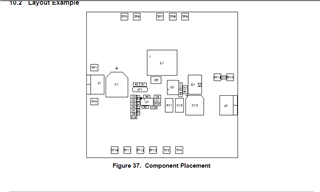
In the above images, you can see the design guide. They have not provided any guidelines for heat dissipation of components mostly mosfet, inductor, and Schottky diode which dissipates significant power.
As my module is 150W, my module generates significant waste power which results in a large amount of heat.
As all components are SMD, I can emit limited heat by mounting a heatsink on them.
I have two to three ways to radiate this heat in the surrounding by increasing copper area, thermal vias, and increasing copper width.
If I increased the copper area of the switching loop and outer loop (where the inductor, mosfet, and Schottky diode are located ) it may radiate a significant amount of heat but at the same time, it becomes a big hotspot for EMI radiation.
So please provide me the solution for both reducing heating and EMI effect BOOST CONVERTER.

