Other Parts Discussed in Thread: TPS54526
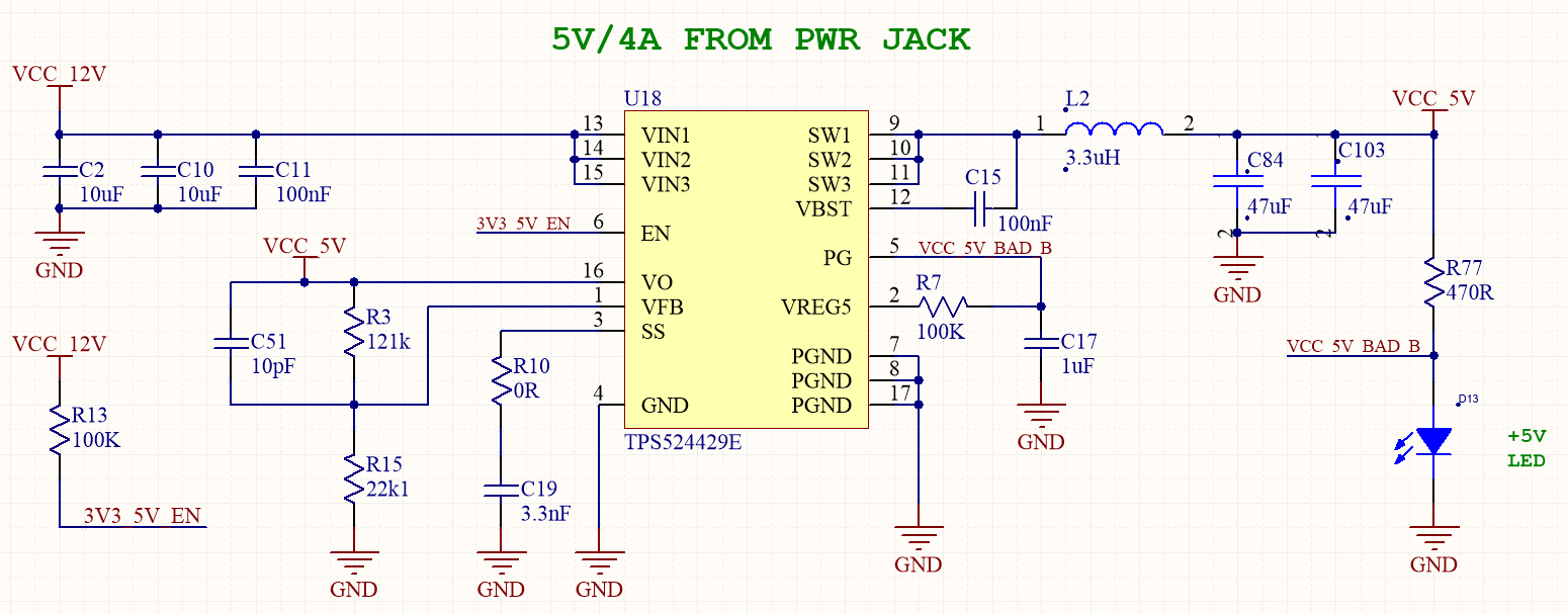
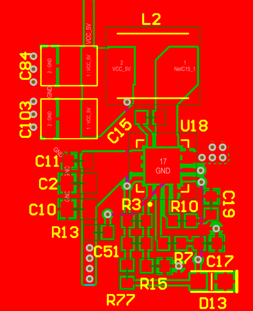
I've decided to use a couple of TPS54429E buck converters in a new design and I just wanted to get some guidance on my layout since I've use the QFN part which does not have a recommended layout shown in the datasheet. The schematic and layout are shown below, I've got the 12V power coming in from the bottom, and 5V exiting at the top. I plan to use the same part for a 3v3 rail, and will likely use an identical layout but with different values for some components.
I'd really appreciate if someone could have a look at my layout and let me know if it is going to be adequate. I've done my best to folow the layout guidelines, but could do with a sense-check to make sure I've not missed anythnig significant in this first draft. The PCB will be 4 layers, with a ground plane directly below the top layer.
Thanks.