This thread has been locked.

If you have a related question, please click the "Ask a related question" button in the top right corner. The newly created question will be automatically linked to this question.

UCC24612: ideal diode (LM74700 ( LM7480 ) )

Part Number: UCC24612
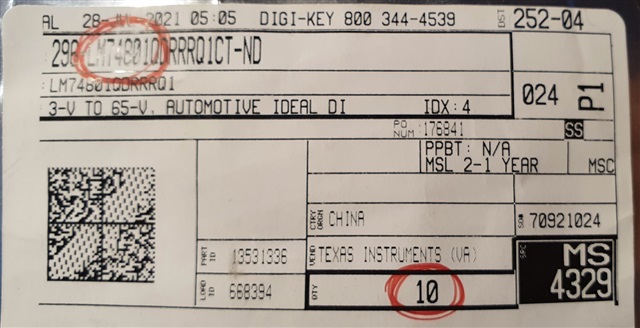
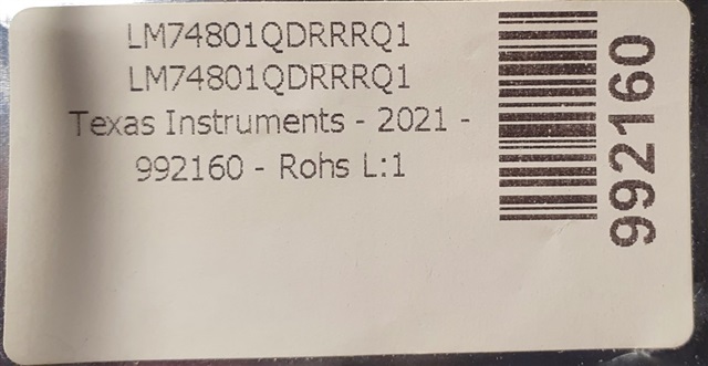
Other Parts Discussed in Thread: LM7480, , LM74800-Q1, LM74700-Q1, LM74800EVM-CD, TPS2411

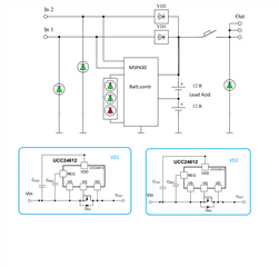
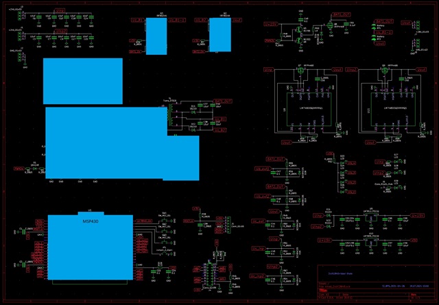
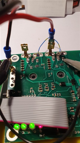
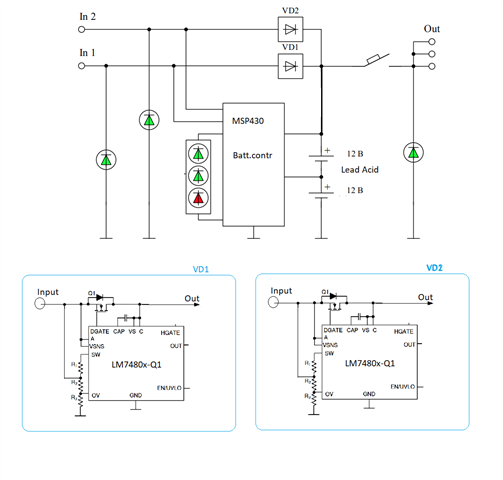
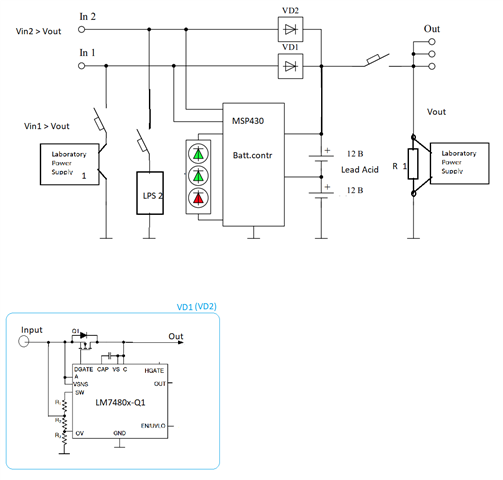
I need to develop an uninterruptible DC power supply circuit, with a voltage of 20-30 volts. The scheme is shown in the figure.
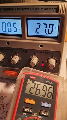
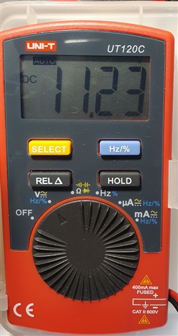
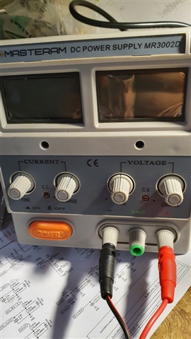
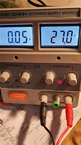
The problem is that I do not have a pulsed power supply, only direct current. The current is assumed to be 2-25Amps, so the use of Schottky diodes will lead to large heat losses. That's why I chose the "ideal diode" solution.
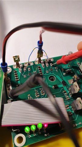
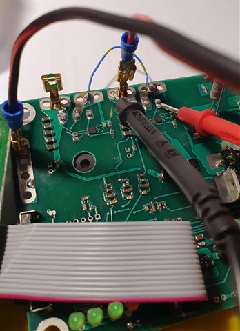
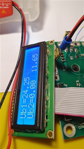
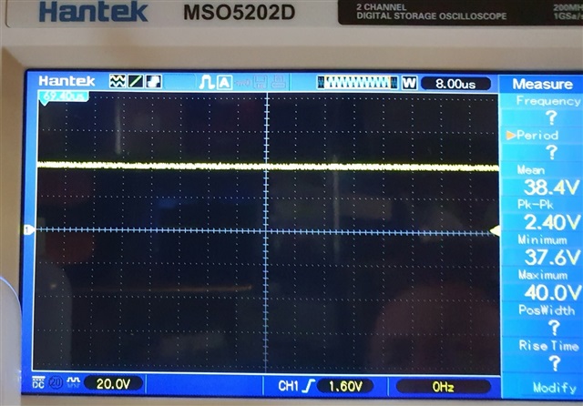
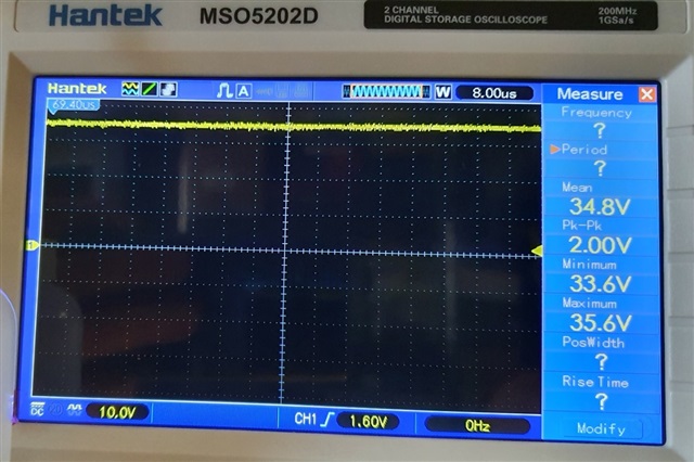
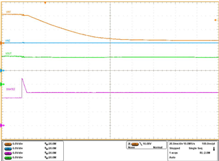
But then the problems started ... Initially, I assembled the circuit on the LM74700 ( LM7480 ) and the circuit works fine, but only if there are no batteries at the output (see my diagram). The battery has its own voltage, and the circuit leaves the field-effect transistors on even if power is lost at input 1 or 2. If power is lost at input 1 (for example), there is still voltage at input 2, because the circuit “sees” the voltage that it itself broadcasts from its output through an open field effect transistor. There is a danger of potential equation currents flowing between input 1 and input 2 in case of incomplete loss of voltage, or even battery discharge on the input 1 or input 2 circuit.
So I want to use the ucc24612 (as in my schematic) as an "ideal diode".
I did not find a similar circuit in the datasheets, and did not find a mention that this will only work on direct current.
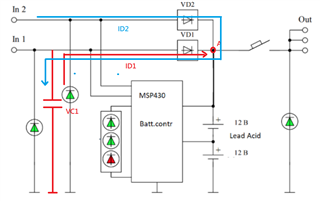
I don't really understand how the ucc24612 works using just one power wire.
If I connect power to the ucc24612 from the output of the circuit (where I have batteries) then I get the same problem: the FET will always be open because the batteries transmit their voltage through the open transistor to input 1 (2).
I ask you to help me understand and how can I solve my problem.

  • Hi, Alexander:

    Thanks for asking.  Would you please share me if there any input capacitor of IN1 and IN2?

     UCC24612 turns on and off according to VDS voltage. Please refer the figure shows below. UCC24612 turns off when ISD*RDS is higher than -9mV.  So if the power lost IN1, (ID2-ID1)*RDS is not over -9mV. MOSFET would not be turned off. 

    Thus, would you mind the check the VDS, ISD and VGS voltage waveform in your condition? It provides the clues to see what happen here. 

    Frankly speaking, UCC24612 might not a good solution to this kind of application. It is designed to be a SR controller of flyback converter. For example, UCC24612 has min-on time and min-off time. IC keeps its status (on or off) no matter the IN1 or IN2 varies.

    Regards,

    Wesley

  • Thanks for your reply.

    yes, power supplies can be used as inputs, which have capacitors at the output, so the voltage at input 1 or 2 can drop slowly.

    There is a problem with this. I made a circuit on the LM74800 (figure below). The circuit remained always on (the FET transistor is always on) if the voltage at input 1 or 2 was lost. I see that the main problem is that there is a battery at the output of my circuit. The second problem is that you need to provide two inputs. But if there is a second voltage, when the first one disappears, the first input circuit still remains on.

    I hate to use schottky diodes, but this seems to be the only solution... Do you have any ideas how to fix this?

  • Hi, Alexander:

    I saw there is reverse current protection of LM74700 (LM7480). So basically, when current or polarity reverse, LM74800 should be protected. 

    I think the question should be the MOSFET RDS you chose.  As the reverse current blocking is -4.5mV of LM74800. So the MOSFET is IRFP4460 (2mohm). 

    So the protection is triggered when Ireverse is 2A around....

    I am sorry I am in charge ACDC products. I would look for other expert's help to check this thread.

  • Thank you for your responses.

    I myself used solutions with synchronous rectification in AС-DC converters. (IR1167 for example). I have serial products (hundreds of pieces produced) in which 450W synchronous converter 230v - 15v. With impulse modes, everything is clear and predictable for me.

    The problem arose when designing the circuit to operate only on direct current. When operating on direct current, there is no such obvious decrease in voltage and voltage "through zero". I thought I could solve my problem (uninterruptible power supply) by using an "ideal diode", but when I assembled the circuit (soldered) with the LM74800, I was very surprised that the circuit continued to keep the FET transistor open even after the input1 voltage was lost.

  • Hi Alexander,

    I can help you with queries on LM74800-Q1. Let me go through this conversation and get back to you with my comments on issue observed by tomorrow. 

  • Hi Alexander,


    LM74700-Q1 and LM74800-Q1 are Ideal Diode controllers which have reverse current blocking functionality. Considering LM74800-Q1, when ever output voltage goes above the input voltage by V(AC_REV) = 4.5mV, the DGATE is turned OFF.

    This means the reverse current required to trigger DGATE turn OFF is = V(AC_REV) / Rds(on).

    These devices also have linear gate control architecture. This control scheme ensures 0A reverse current for slow variations in input/ output voltage. 

    In your test case where Input1 is removed and Input2 is present, the DGATE of the LM74800-Q1 in the path of Input1 should be turned OFF. It is surprising to know that the DGATE is not turning OFF. Can you please share waveform captures with signals (IN, OUT, DGATE, CAP) captured during this test condition. 

  • I'm talking about my scheme and my experiences.

    1) scheme (_u0.jpg)

    The block diagram (general idea) is the same as in my first post. That is: two voltage inputs, through two "ideal diodes" should go to the output, and at the output there is a 24-volt battery. General idea: uninterruptible power supply, two independent inputs, one output with a battery.

    2) 2) My laboratory power supply (LPS) and my multimeter.

    3) I connect the batteries to the output (Uout) of my circuit. The microprocessor does not work, the LCD screen does not light up. LPS is off. Everything is fine.

    4) I turn on the LPS and set it to 27 volts (this voltage is higher than on batteries). Batteries start charging with low current (10-20mA). The ideal diode circuit is put into operation.

    5) The scheme is in operation. The voltage at the "gate" of the FET transistor of an ideal diode is relative to the "ground".


    voltage between S and G FET transistor :

    This means that the ideal diode control chip has fully opened the FET transistor.

    6) I turn off the LPS. (I can also turn off the wires, the effect does not change).


    7) I take measurements: The voltage between the "S" and the "Gate" of the FET transistor remains the same = 11.23 volts. This means that the circuit continues to keep the FET transistor on, despite the complete absence of input voltage (LPS is turned off). The microcontroller is turned on and powered by batteries.


    According to the datasheet, this circuit should not work !!!
    The microcircuit was supposed to turn off the FET transistor in the event of a power failure at the input. This is not happening.

    If I apply the second voltage (input 2) then I will see that the second channel (control chip of the second channel) will turn on the second channel of the FET transistor, and if  I turn off the second channel, then the second FET remains open (Vgs=11.23 volts). If I turn off the first channel, then I get two FETs turned on and the whole circuit continues to work on batteries!

    This is madness... Disappointed

  • Hi Alexander,

    Can you please share waveform captures on oscilloscope (instead of the multimeter readings)  with signals (IN1, OUT, DGATE1, CAP) captured during this test condition. 

  • I don't have a multichannel oscilloscope. I can only take one signal.

  • Here is Vgate's signal to ground.
    when voltage is supplied from the power supply.

    And this is the Vgate signal with the power supply turned off, the power comes from the battery. (Batteries).


    When switching the power supply (disconnecting the input voltage), the line on the oscilloscope just goes down, no pulses, no spikes. Just the same straight line but a little lower (look at the last photo). There is no break.

  • Hi Alexander,

    Thanks for sharing the scope shots but Ideally we would like to have all the 4 signals captured in one scope shot as it would be easy to debug. I was interested in knowing the voltage on the Input, Output, VCAP

    1. What is voltage at the input (Vinp) when the LPS is turned OFF or disconnected ?
    2. Can you redo the same test with a 100 kohms resistor connected across IN_GND ? (If there is a non zero voltage on the input, wait for it to discharge)
    3. Also, change the connection of  EN/UVLO resistor ladder from Vout to Vinp. 
    4. Are you using LM74800-Q1 or LM74801-Q1 in your circuit ?
    5. Is it possible for your to change the routing on the board for VS pin ? Can you connect VS pin to A or Vinp instead of C or Vout ?
    6. Also, just wanted to know,
      1. How many boards have you build and tested ?
      2. Do all the boards show the same issue ? 
      3. Did you try replacing the IC on the board with a new one ?

  • You write : "... Can you repeat the same test with a 100 kΩ resistor connected to IN_GND? (If there is a non-zero voltage on the input, wait for it to discharge)..."

    I repeat to you: I cannot do this, because even if I completely break the circuit from the LPS (power supply), there is still voltage at the input! This voltage is equal to the battery voltage. (see my pictures above in the last post). I wrote that due to the fact that the FET transistor remains open, and there is a battery at the output, there is always (absolutely always) in this circuit when it is turned off (a physical break in the input circuit), there is voltage and the FET never closes. This is the problem with which I started contacting support.

    You don't read what I write. Please read this thread carefully from the beginning.

    You write : "... How many boards have you built and tested?..."

    My answer: I always test two devices (two boards). Each board has two "ideal diode" chips (circuits).

    "... All the boards have the same problem?..."

    My Answer: yes, the problem is identical. The problem is 100% repeated.

    "... Have you tried replacing the chip on the board with a new one?..."

    My Answer: I tried, it does not help, the problem is 100% repeated.


    "...Also, change the connection of the EN/UVLO resistor ladder from Vout to Vinp...."

    My Answer: It doesn't help! because the FET transistor remains open and the voltage from the output is transmitted to the input of the circuit. See my real board and schematic.

  • You can repeat my experience yourself.

    For this you will need: LM74800 Evaluation Module: LM74800EVM-CD

    www.ti.com/.../slvubu3a.pdf

    You will get 100% repeat my problem.
    The main condition: batteries must be used as a load, as in my diagram (the first post of this topic).

  • Hi Alexander,

    LM74801-Q1 has only comparator based reverse current blocking. For LM74801-Q1 to detect a reverse current and turn OFF the FET, there has to be a reverse voltage of -4.5 mV across A-C pins. The reverse current required for LM74801-Q1 to detect a reverse current while driving IRFP4468 is 4.5mV/2mΩ = 2.25A.

    I see that there is significant capacitance on the input. When the input power supply is removed/disconnected there is no path for the input cap to discharge. As long as the reverse current flowing from OUT to IN is less than 2.25A, the LM74801-Q1 would not detect it. In your case, this is what is exactly happening - While the input is removed, the reverse current required to charge the input cap voltage equal to that of the output voltage is less than 2.25A. So, the DGATE is not turned OFF. 

    This issue can be resolved by using LM74800-Q1 instead of LM74801-Q1.

    • LM74800-Q1 has linear gate regulation scheme in which the gate voltage is controlled as a function of load current. As the load current reduces close to 0A, the Gate of the FET is also pulled low to turn OFF FET and block reverse current flow. 
    • Also, as mentioned before, consider connecting the EN/UVLO resistor ladder from Vout to Vinp as this resistor ladder would act as load for the input caps to discharge. Once the input is discharged, the EN/UVLO would also be below its threshold which would disable the device (additional protection apart from reverse current blocking).  

    It would have been easy to find the root cause had the schematics showed up LM74801-Q1 instead of LM74800-Q1.Hope you understand that without waveforms it is not easy to comprehend the test conditions and voltages at each pin in different test conditions. 

  • I get the impression that you are mocking me... Disappointed

    You write: "...I see that there is significant capacitance at the input. When the input power supply is removed/disabled, the input cap cannot discharge...."

    My answer is written above, and I repeat it: even if I remove all the capacitors from the input, then when the voltage is turned off from the input, the voltage from the batteries remains at the input, i.e. at the input all the same(!) There will be an output voltage (battery voltage).

    Before I applied the LM74801 chip, I tried to solve this problem using two voltage dividers and an MCP430 ADC - this problem was not solved in any way! For the reason that I described: the FET remains open, because the potential (voltage) from the batteries continues to flow to the input of the circuit through the open FET transistor. The ADC does not see the difference between the input and output (potential, voltage is the same) and the MCP430 cannot decide to turn off.

    Using the LM74800 will not solve anything, because the problem (opened once FET) remains. The problem is not solved by the use of the UCC24612 for the same reason: the presence of a battery voltage at the output of the circuit! potential (voltage) from the batteries(Uout) continues to flow to the input of the circuit through the open FET transistor.

    The application of the LM74800 is similar to that of the UCC24612 because they both have proportional gate control (see datasheet). I tested the circuit with the UCC24612 and got 100% the same problem: once the FET is opened once, it will never close again as long as there is voltage on the batteries present.

    You can easily repeat my experience if you take two LM74800EVM-CD (LM74800-Q1 ideal diode controller evaluation module) circuits and connect them as in my circuit. The main condition: there must be a battery(accumulators) at the output of the circuit.

    If you don't want to see the problem, and that the problem is inside the chips, I want you to bring in an Engineer with more circuit experience than you. You do not realize that the problem is not in the divider resistors and not in the capacitors, but in the principle of the "ideal diode" circuit.

    There is no problem, and everything works as written in the datasheets, only(!) under one condition: there should be no batteries at the output! I checked it many times.

    Without batteries, the circuit turns off the FET transistor if the voltage disappears from the input. But if there are batteries present at the output in the circuit, then the FET opens once (the first time) and does not close again, because there is no one to turn it off. The circuit itself provides the input voltage by broadcasting it from the output.
    Check this fact (experience described by me above in previous messages) yourself, please, before you write me an answer. I have been doing power electronics for decades and I write what I see in the circuit on my desk. Practice shows that the "ideal diode" circuit does not work if there is a battery at the output of the circuit.

  • Hi Alexander,

    Sorry if I have hurt you in any way. I didn't mean to disregard you. 

    Regarding this issue, This is a common problem we have seen with customers using 'only comparator' based ORing controllers (like LM74801-Q1 or TPS2411) in ORing applications. I would recommend you to please test with LM74800-Q1 and share the observations with us. 

    LM74800-Q1 has the same linear gate control as that of LM74700-Q1. Please refer to LM74700-Q1 datasheet  (Figure 10-12 to Figure 10-17) for ORing related waveforms. You can expect similar results with LM74800-Q1.

  • This scheme will not work either. The reasons are described by me above.

  • I can share the test results with LM74800-Q1 in ORing configuration by end of this week. We will see that when the Input1 power supply is removed, the Gate of LM74800-Q1 in the power path 1.

    You can also check the same in your circuit using LM74800-Q1.

  • I asked you not to write me an answer until you yourself, with your own hands and eyes, see what I see.

    The LM74800-Q1 won't solve the problem, your (Texas Inc.) "ideal diode" ICs have the same driving principle.

    The voltage at the input of my circuit will still be present, after the first turn on of the FET transistor, if the battery voltage is present at the output. LM74800 and LM74801, according to the datasheet, allow you to use the circuit as I wrote above.

    The problem is that when the input is turned off, the same reverse voltage of 4.5mV does not appear, which is necessary to turn off the "gate" control circuit. The voltage on the "gate" of the FET decreases but does not disappear completely.

    I will wait until the end of the week when you can repeat my experience.

    P.S. Not only you have a similar problem, the LTC4358 has the same problem (if there is a battery in the output).

  • Sure.. I can get back with test results.

  • Hi Alexander,

    Please find test results below,

    Test Condition:

    • 2xLM74800-Q1 in ORing configuration, 
    • Vin1 = 12.5V, Vin2 = 12V,
    • Vin1 Removed

    Signals Capture1: Vin1, Vin2, Vout, DGATE1

    Signals Capture2: Vin1, Vin2, Vout, DGATE2

    As described earlier, you can see that as Vin1 is removed,

    • Vin1 starts to discharge
    • DGATE is immediately turned OFF (DGATE-A shorted internally)  when Vin1 goes below Vin2
    • Vout is now supplied by Vin2

  • Are you using a circuit simulator?
    I don't use a simulator! I'm using a real working circuit.

    You spent not my experience!
    You checked the operation of switching Input1 and Input2 without taking into account the fact that there is a battery at the Output! This is not my experience.
    You've done the wrong experiment.
    My experience is described in my post above.
    Input voltage = 27 volts. Battery voltage (at the output of the circuit) = 24.6 volts.
    The battery is always connected to the output (see my diagram).


  • Hi Alexander,

    This is not a circuit simulator result. This test is done in Lab bench using Evaluation modules. 

     Isn't switching from Vin1 to Vin2 same as switching between Vin1 and Battery ? Why do you think using a Battery at the output will be different than having a power supply (Vin2) connected at the output when Vin1 is removed ?

  • You write : "...Isn't switching from Vin1 to Vin2 the same as switching between Vin1 and Battery?..."

    My answer: Not the same.

    The battery at the output of the circuit does not allow the voltage at the output of the circuit to drop quickly and sharply. The logic of the circuit (your logic) is broken if the battery is connect at the output (Vout) of the circuit.

    You didn't repeat my experiment. In your case, you did not get the same result as mine.

    Do as I wrote:

    1) We connect the battery to the output of the circuit (Vout).

    2) We apply a voltage higher than on the battery to the input of the circuit (Vin > Vout).

    3) We observe that the control circuit has worked (FET has opened or half opened).

    4) Turn off the input voltage (switch off).

    5) See (observes) the voltage at the input of the circuit, equal to the voltage on the battery, i.e. The battery powers the input circuit, the FET-diode didn't cut the circuit...

    If you don't have a battery, you can simulate one.

    Power supply + load on it, and connect to the output of the circuit. See my picture.
    The resistor (R_1) must be of high power so that it does not burn out when current (input voltage) is applied from the power supply. It can be an incandescent lamp (halogen lamp from a car) or a lamp from a table lamp. 10-20W of power.


    Attention! Do not use the same power supply for three voltages! There must be a galvanic isolation between the primary network and the secondary network. The circuit assumes three independent power supplies.

  • Hi Alexander,

    I will try to see if we can do this experiment in lab. Meanwhile are you willing to test LM74800-Q1 on your board ?

  • with LM74800 Nothing will change.

    I will now tell you what is the "root of the problem". The root is in the application of FET transistors.

    Unlike the "bipolar transistor", the FET is a "voltage controlled" device. Here are some pictures of FET work.

    From full off to full on.

     The FET is more of an "adjustable resistor" as opposed to a "bipolar transistor" which has clear NPN junctions.

    So, all your (Texas Inc.) microcircuits of the "ideal diode" cannot completely turn off the FET, because for this it is necessary not only to remove the voltage from its "gate", but also to discharge the "gate", but it is better to send a negative impulse to it voltage.

    This is a radical problem with chips and my circuit.

    My circuit cannot be implemented in this form...

    You should inform the designers of these ICs that there is a use case that cannot be implemented (my circuit with a battery output). You should warn IC users that this problem exists and that users may experience problems due to voltage drop from the output to the input of their circuits. This can lead to accidents...

    The only correct (almost correct) answer was given by your employee Wesley Hsu . For which I am very grateful to him, he understands what the problem is.

    I'm still waiting for your advice: how can I change the circuit so that I get the functionality (two ideal diodes) that I want?

  • Hi Alexander,

    I am sorry but I do not agree with you. 

    Our ideal diode controllers short the Gate and the Source pins internally to turn OFF the Mosfet. By pulling down the gate to source voltage of the Mosfet to 0V, The Mosfet turns OFF and blocks any current flow Drain to Source due to its high impedance (open circuit).  This is how reverse current is blocked when the gate is pulled low.

    We have provided you with enough evidence (waveforms in LM74700-Q1 datasheet + waveforms shared in previous messages) to show that in ORing configuration, when Input power supply is removed, the Input voltage is not charged from Output when you use a linear Gate control device like LM74800-Q1.

    If you are unwilling to accept these results shared and test LM74800-Q1 in your circuit, there is nothing much we can do to support you further. 

    Thanks for reaching out to us and have a good day!