


Hi.
I'm accessing the DF (data flash) via I2C, as per the recipe in bq35100 Technical Reference Manual (Rev. C) (ti.com), "12.1.1 Read from DF Example:
1. Write 0x00 0x40 (DF address in little endian format) to ManufacturerAccessControl(0x3E, 0x3F).
2. Read ManufacturerAccessControl(0x3E, 0x3F) to verify.
..."
(In my case the DF addr. is 0x4010 (Vin gain).)
I found a problem with this I2C command sequence when the clock frequency of the microcontroller I'm using was boosted (x6).
What happened was that the value read back was no longer 0x4010 (in my case it was 0x00A4), and so the verification was failing.
After some investigation I found that a delay is needed between steps 1 and 2. (I think that without this the read is actually a Quick Read and so is linked preceding operation.)
The delay amount is more than 200uS. I looked in the BQ35100 datasheet and a poss. relevant spec. point is tBUF, bus free time between stop and start, but this is 66us.
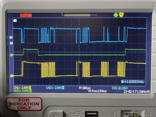
Attached photo's: SCL & SDA in yellow & light blue; the light green is the gap between the I2C op's.
(1) Working case - 200uS gap
(2) Not working - 100uS gap.
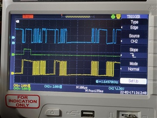
(Beside the different last 2 bytes, I also noticed that in the 2nd one, the sending of the device address (read) + 0x3E (MAC reg.) comes sooner as well.)
So I'm wondering if I'm missing something here? Is it that the tBUF figure is for 400kHz but I'm using 100kHz and so it is 4x longer in this case?

