Hi team,
We received PCN.
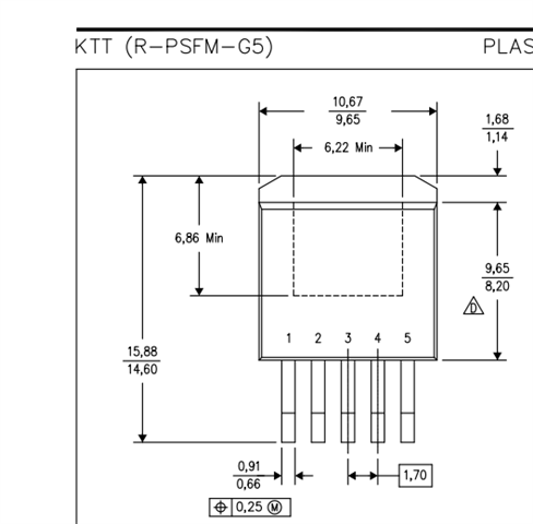
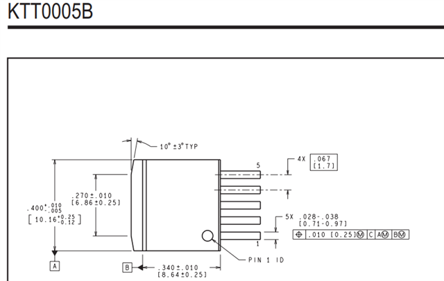
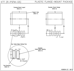
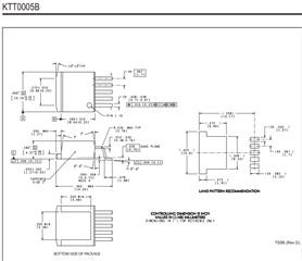
PCN said Package Outline Difference.
In that comment, it says that shift component placement by 1.8mm towards the lead solder pad.
Looking at the board layout, I think it can be implemented without shifting as it is, is this my understanding correct?
Sincerely.
Kengo.

-
Ask a related question
What is a related question?A related question is a question created from another question. When the related question is created, it will be automatically linked to the original question.