This thread has been locked.

If you have a related question, please click the "Ask a related question" button in the top right corner. The newly created question will be automatically linked to this question.

TPS65132S: question about tps65132xx enable and disable operation

Part Number: TPS65132S
Other Parts Discussed in Thread: TPS65132, , USB2ANY

Dear TI,

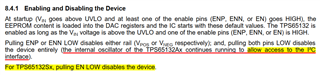
I found below description in tps65132xx datasheet. It said that for tps65132A, pulling both ENP,ENN low will disable the device but the I2C can still communicate with tps65132A.

My question is for tps65132S, if the only EN pin is pulled down, is I2C of tps65132s still accessible? 

If the answer is NO. Does it mean that I have to pull EN pin high firstly and than write the configurable registers like reg0x01,02 for positive and negative output voltage, and reg 0x02, reg03 for the power-on and power-down sequence control?

If my understanding is right, it seems a little strange for me, because if EN pin is pulled high, Vpos and Vneg will have outputs immediately without delay as the default value of reg0x02 and 0x03 configs. Then we can not realize the power-on sequence and delay time we want. I doesn't make sense.

But when I pull EN pin low on tps65132S EVM, I cannot connect to the it with USB2ANY tool and GUI. 

Look forward to your feedbacks, thanks. 

  • Hello,

    In the TPS65132 product family, TPS65132A and TPS65132A0 are the only devices that continue to provide access to I2C register when ENP/ENN signals are both de-asserted. Other devices in this family, including TPS65132S, do not have the I2C interface active when EN (TPS65132S) or ENP/ENN are de-asserted. That is the reason that TPS65132A/A0 have a much higher shutdown current compared to other devices in the family.

    Kind Regards,

    Liaqat

  • Hi  Liaqat,

    Thanks for your reply. So it is clear if the  EN pin of tps65132s is pulled down, the I2C interface is not accessible.

     Then it seems a little strange for me, because if EN pin is pulled high, Vpos and Vneg will have default output value(+/-5.4V) and power-on sequence(no delay) immediately as the default value of reg0x02 and 0x03 configs. Then how can we realize the power-on sequence, specific delay time and voltage value we want at the beginning of output rise. Thanks.

  • Hi Jiayu,

    Any specific output voltage values that the application needs can be programmed into the device eeprom during manufacturing test at first power up and once values are burned into eeprom, device will come up with new voltage and delay sequence during subsequent power ups. It is correct that at first power up during manufacturing test, the device will come up with default voltage at output rails.

    Kind Regards,

    Liaqat