This thread has been locked.

If you have a related question, please click the "Ask a related question" button in the top right corner. The newly created question will be automatically linked to this question.

LM5176-Q1: Calculation method of lm5176 power consumption

Part Number: LM5176-Q1
Other Parts Discussed in Thread: LM5176, CSD18532Q5B

ALL HI!

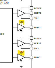
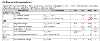
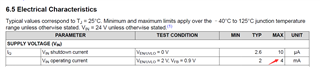
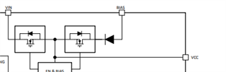
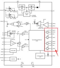
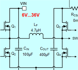
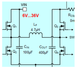
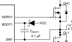
At present, lm5176 is used to design the circuit, with input of 8 ~ 36V and output of 12V / 12a. Two upper tubes and two lower tubes are used in parallel to form buck and boost circuits.How to calculate the power consumption of lm5176 itself at the maximum output power. thank you! The power consumption of lm5176 is the sum of the power consumption of VIN and VCC?

  • Hi Sheng,

    thank you for using the E2E forum.

    When calculating the power consumption of the LM5176 you need to consider several aspects:

    Loss on the internal linear regulator: is the consumed current multiplied by the input voltage - the Vcc voltage

    Note: Vin can also be replaced by Vbias - depending on application - please check

    current:

    1) logic operation current - see datasheet: VIN operating current

    2) current for low side FET drivers

    Current required for driving the output drivers.

    - loss on driver resistance (check for drive high and drive low) based on the current required to drive the external FET

    - for the high side driver this current is supplied by the internal Vcc linear regulator (so this needs to be added for this as well - see above)

    Best regards,

     Stefan

  • HI!  Stefan!

    Thank you for your reply!

    My understanding is that the power consumption of lm5176 includes the sum of VIN and VCC power consumption. Vin can be replaced by Vbias power supply. Vin is used to drive the low-end field tube and the logic power supply inside the chip, while VCC is mainly used to drive the high-end field tube. According to which current is VIN calculated? Is it operating current according to VIN in IQ? Maximum 4mA? The current driving the field tube is ihdrv1,2 and ildrv1,2 current?Can you provide the calculation formula and parameters?Is it calculated according to the current parameters indicated by the arrow in the figure below?

  • HI Sheng,

    Vcc is used to drive the low side driver as you can see from below figure from the datasheet:

    The supply for the high side is generated by the small external charge pump (Diode / C ) on SWx and BOOTx

    Best regards,

     Stefan

  • HI!  Stefan!

    Can you list the specific calculation formula?

  • What is the maximum current consumed by the internal linear regulator? How to determine this?As shown in the figure below, is it 4mA or 65mA? Or how much current?

  • The above logic working current is calculated according to 4mA?If Vbias is used instead of VIN, what is the current?

  • Hi Sheng,

    the current is the same but the losses in the linear regulator will be different.

    please not that Vcc will be regulated to 

    this means the the voltage on the linear regulator (Vin or Bias side) multiplied by the current will show up as losses in the device.

    So it depends on which path is used and what is the voltage level there.

    Best regards,

     Stefan

  • HI!  Stefan!!

    As shown in the figure below, the power consumption of the driving part of lm5176 is calculated according to the current and resistance in the figure? P=I2R?How does the driving power consumption of lm5176 distinguish between full load and no-load output?

  • Hi Sheng,

    not sure about your question.

    The output driver for the external MOSFET does not distingue between different load conditions. It the devices adjusts the duty cycle of the gate driver signals.

    Best regards,

     Stefan

  • HI!  Stefan!!

    Is it how to calculate the power consumption of the upper and lower tube driving circuit in the figure below?

  • HI!  Stefan!!

    How is PD calculated in the figure below? I use the design function of TI official website to obtain power consumption.

  • Hi Sheng,

    you can use following formulas:

    Switching Current 

    =(Vin-Vdd)*Fsw*(Qg_Q1+Qg_Q2)+(RHDRV1,2pullup+RHDRV1,2pulldown)*Fsw*Qg_Q1*Vdd/(RHDRV1,2pullup+2*Rgate1+RHDRV1,2pulldown)+(RLDRV1,2pullup+RLDRV1,2pulldown)*Fsw*Qg_Q2*Vdd/(RLDRV1,2pullup+2*Rgate2+RLDRV1,2pulldown)

    Switching Current Loss

    Buck: (Qg_Q1+Qg_Q2)*Fsw*Vin;
    Boost:(Qg_Q3+Qg_Q4)*Fsw*Vin;
    BB: (Qg_Q1+Qg_Q2+Qg_Q3+Qg_Q4)*Fsw/2)*Vin

    with this mapping

    Best regards,

     Stefan

  • HI!  Stefan!! 

    VDD is the output voltage of the internal linear regulator?

    Internal logic power consumption P = (vin-vcc) * IQ (4mA) calculation of lm5176? If I use Vbias as the input voltage, the internal logic power consumption P = (vbias-vcc) * IQ calculation? What is the IQ current value at this time? Note: VCC is the output voltage of the internal linear regulator.

    The driving voltage of Q2 field tube is the output voltage of internal linear regulator (7.35v). What is the driving boost voltage of Q1 field tube?

  • Hi Sheng,

    you are right Vdd and Vcc are identical in this conversation. (Just the source where i took this information used different names).

    So Vdd is the output of the regulator.

    Yes, if VBias is used then vin needs to be replaced by VBias in the above formula.

    IQ is independent of VBias or Vin (as long as the voltage is above Vcc).

    The supply for Q1 is generated by the small charge pump between BOOT1 and SW1

    Best regards,

     Stefan

  • HI!  Stefan!!

    I probably understand the calculation method of chip power consumption. Now let me calculate, please help confirm whether it is correct.

    The design input voltage of the power supply is 8 ~ 36V, but it is usually 24V input, so the input voltage Vin = 24V and the output voltage is 12V / 12A.

    Most of the time, the circuit works in the buck mode, so I first calculate the chip power consumption according to the buck circuit mode.The field tube used in the step-down circuit is csd18532q5b. His Qg= 44nc.

    Calculated according to Buck: (qg_q1 + qg_q2) * FSW * VIN, PD = (4 * 44 * 10 ^ - 9) * 400 * (10 ^ 3) * 24 = 1.689w.(FSW=400K)

    Total power consumption Pt = logic circuit power consumption + drive circuit power consumption. PT=((VBIAS-VCC)*Iq)+1.689=((12-7.35)*4*10^-3)+1.689=1.707W.According to the chip manual, IQ = 4mA

    Then the power consumption of the chip in step-down mode is 1.707w. Is this right?

  • Hi Sheng,

    great, that the information helped to understand the behavior

    Your calculation is correct with one small correction:

    (qg_q1 + qg_q2) =  (2 * 44 * 10 ^ - 9)   not  (4 * 44 * 10 ^ - 9)

    Best regards,

     Stefan

  • HI!  Stefan!!

    According to my circuit design above, the switch MOS tube and freewheeling MOS tube of buck circuit use two MOS tubes in parallel respectively. When calculating power consumption, do not consider four MOS tubes?

  • Hi Sheng,

    thanks for highlighting this, on the first view I missed that, so your formula is correct.

    Best regards,

     Stefan

  • Thank you very much for your support ! Stefan!!