This thread has been locked.

If you have a related question, please click the "Ask a related question" button in the top right corner. The newly created question will be automatically linked to this question.

BQ29209: External Cell Balancing | Datasheet may not be correct

Part Number: BQ29209
Other Parts Discussed in Thread: TINA-TI

Hi,
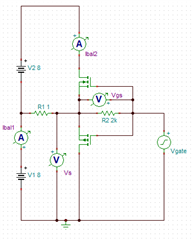
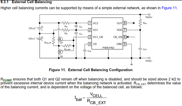
the recommended schematics for external cell balancing might not work like it's intended.
In case of Q1, the Drain Source voltage will be the same as the Gate Source voltage when activated, and because the Source is above the current limiting resistor, the source will start to rise once current starts flowing.
This will start closing the FET and it'll not be in the saturated region anymore.
Same goes for Q2

I believe there should be separate resistors for Q1 and Q2, Q1 drain side and Q2 source side.
Please confirm this, we will manufacture 1k units and I need to add 1A current balancing.

thank you,

Lorand

  • Hello Lorand,

    I would advice you test the device prior to manufacturing. To make sure the circuit works as intended within your parameters.

    According Section 8.1.2 Cell Balancing of the datasheet, the IC performs cell balancing on the cell with the higher voltage. If Cell 2 is being balanced VC1_CB would be pulled to Vdd, for Q1 the gate would be at ~ Vcell1 + Vcell2, while source is at Vcell1. So gate-source voltage would be ~Vcell2. Hence the FET will be On and conducting, the drain-source would be a low resistance so there should not be much of a drop, it would not be the same as the gate-source voltage. The cell balancing current would balance according to Vcell2/RCB_EXT.

    For balancing Cell 1, VC1_CB is pulled to GND. Q2 would be on as gate-source voltage would be -Vcell1. So the balancing current would be Vcell1/RCB_EXT.

    Adding an additional resistance on the drain/source would only serve to further limit the current. Considering you want to balance at 1-A, you may have to use very small balancing resistors with sufficient power rating.

    Best Regards,

    Luis Hernandez Salomon

  • HI,

    I don't believe what you're saying is right.
    If Cell 2 is being balanced:
    -- VC1_CB would be pulled to Vdd, for Q1 the gate would be at ~ Vcell1 + Vcell2  <- AGREED
    -- while source is at Vcell1 (I believe you mean Vcell1, not Vcell2) <--- I don't think so.
    The moment balancing current starts to flow, Source of Q1 is going to be Vcell1 + RCB_EXT * Ibal.

    Another way to think about this is approaching it is reductio ad absurdum. Let's assume VdsQ1 is indeed very low because it is in a low impedance state (RdsonQ1 verysmall). That also means that The source is at Vcell1 + Vcell2 - RdsonQ1 * Ibal ~= Vcell1 + Vcell2. At the same time VgateQ1 is also ~ Vcell1 + Vcell2, which means that Vgs would be almost 0V. This is a contradiction

    same on the lower side.

    Lorand

  • Hello Lorand,

    I gave it some more thought.

    I briefly simulated both scenarios, and it seems to be working. The source voltage was roughly Vcell1. However, I understand your points.

    I do not really understand how it exactly is working, as I arrived to the same conclusion you did after reading your comments and after giving it some more thought. So it is a bit confusing and we may be missing something.

    Even though the datasheet circuit seems to work, I will say that your original comment of "I believe there should be separate resistors for Q1 and Q2, Q1 drain side and Q2 source side." would also work correctly, I've seen similar things in previous designs (like in this thread https://e2e.ti.com/support/power-management-group/power-management/f/power-management-forum/748250/bq40z50-r2-external-cell-balancing-connection-for-cell-1)  I would say to do this instead, it should be less confusing and you should have the voltages more defined.

    I hope this helps. Let me know if there is anything else. I will also ask another person in the team to see if they have any further comments.

    Best Regards,

    Luis Hernandez Salomon

  • I wanted to simulate it as well but could not find the part in Tina-TI. Do you have a spice model available for the part somewhere?
    Agreed, I think the separate resistor solution would work as intended, would be really curious about the simulation though.

    Is there an eval board for this part, I wasn't able to find one but saw some Chinese sites discussing "BQ29209EVM Evaluation Module"

    thank you,
    kind regards,

    Lorand

  • Hello Lorand,

    I do not have SPICE model of the part.

    I just placed the external circuit as shown in the datasheet and in your picture and assumed the gate voltages based on the Functional Block Diagram in the datasheet. Where the gate is pulled to Vdd if Q1 is on or if it is pulled to GND if Q2 is on.

    This is not a very accurate simulation, I used generic MOSFETs, which had high thresholds (Couldn't find any with low thresholds), so I adjusted the voltages to make it work just to see the general behavior of the current path and voltages.

    This part released over 10 years ago, so I believe we stopped selling the EVMs for this part, I apologize. 

    Best Regards,

    Luis Hernandez Salomon