Hi,
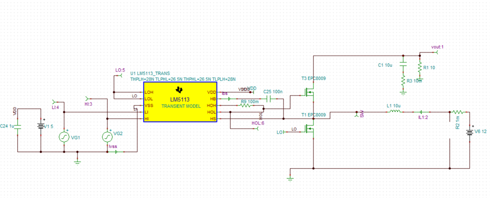
I am working on a TINA simulation to use LM5113 for driving a synchronous boot converter.

The circuit is working fine and i am able to generate an output voltage.
But i am interested in understanding the bootstrapping current path.
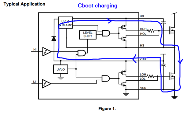
I believe that the bootstrapping capacitor C25 should be charged by the 5V Vdd supply when bottom switch is on.
However, i see a large current entering the Vss pin (IVss) which matches the bootstrapping current (Ibs) when the bottom switch is turned on.

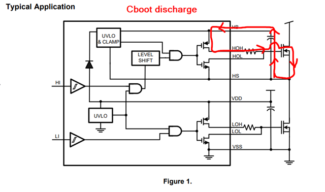
Comparing this result to the internal block diagram of LM5113 i am not able to follow the bootstrapping current path. Can you please explain why i am seeing large current input in the Vss pin.
Additionally, as already mentioned in multiple threads (https://e2e.ti.com/support/power-management-group/power-management/f/power-management-forum/490283/lm5113-falling-edge-spikes)
i am seeing falling edge spikes that does not make much sense.
I am attaching my Tina Simulation with this thread for reference.
Thanks
Ankit


