This thread has been locked.

If you have a related question, please click the "Ask a related question" button in the top right corner. The newly created question will be automatically linked to this question.

LM5066I: Some devices measure strange values after enabling the output

Part Number: LM5066I
Other Parts Discussed in Thread: LM5066

Hello TI experts!

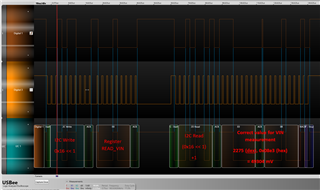
I have a board with a DCDC converter with adjustable output voltage and three LM5066i, each can enable one different output. The circuit of theses are mostly identically with the circuit in the datasheet and only differ in terms of I2C address and UVLO resistors. These three LM5066i are managed by one STM32 and communicate via I2C. I'm now having a problem when reading the value of the register READ_AVG_VIN (DCh) or READ_VIN (88h) as soon as the enable pin (pin 7, UVLO/EN on LM5066i) is set to a high value.

When a voltage of less than ~41 V is applied to the three LM5066i, it is measured correctly no matter if any of the LM5066i is enabled or not.
When a voltage of more than ~41 V is applied to the three LM5066i, it is measured correctly on two of the LM5066i, no matter if enabled or not.
When a voltage of more than ~41 V is applied to the three LM5066i, it is always measured wrong on the same LM5066i (I2C address 0x16) as soon as the enable signal is set. This means, that the measured value always shows ~41 V, even when the actual voltage is higher.

I tried different boards with same assembly and same firmware and some do show this behavior, some not.

Measured value in register READ_AVG_VIN on board 1 (with error):

LM5066i (0x16) LM5066i (0x15) LM5066i (0x50)
~41 V voltage, no LM5066i enabled ~41 V ~41 V ~41 V
~41 V voltage, any LM5066i enabled ~41 V ~41 V ~41 V
~49 V voltage, no LM5066i enabled ~49 V ~49 V ~49 V
~49 V voltage, LM5066i (0x15) or (0x50) enabled ~49 V ~49 V ~49 V
~49 V voltage, LM5066i (0x16) enabled ~41 V ~49 V ~49 V

Measured value in register READ_AVG_VIN on board 2 (without error):

LM5066i (0x16) LM5066i (0x15) LM5066i (0x50)
~41 V voltage, no LM5066i enabled ~41 V ~41 V ~41 V
~41 V voltage, any LM5066i enabled ~41 V ~41 V ~41 V
~49 V voltage, no LM5066i enabled ~49 V ~49 V ~49 V
~49 V voltage, LM5066i (0x15) or (0x50) enabled ~49 V ~49 V ~49 V
~49 V voltage, LM5066i (0x16) enabled ~49 V ~49 V ~49 V

This problem only occurs on some boards and LM5066i devices and I was not yet able to track it down completely. My first guess was that custom register settings have been made on the affected LM5066i. But then again, I do not know which settings are stored in an non volatile memory on the LM5066i and I also do not see any settings that might modify the measurement or calculation of the voltage measurement depending on the state of the EN-pin.

Any ideas?

Best regards,

Christian Wächter

  • Hi Christian,

    Thanks for reaching out. It looks like very strange to me also. Did you check the difference in the raw hexadecimal data?

  • Hi Avishek,

    thank you for your quick response.

    I had a look at the raw hex data and this looks like this:

    Raw data of READ_AVG_VIN (DCh) before setting the enable: 2271 (dez), 100011011111 (binary)

    Raw data of READ_AVG_VIN (DCh) aftersetting the enable: 1926 (dez), 11110000110 (binary)

    Unfortunatelly this did not help me to understand the problem. Currently I'm checking the I2C signals.

  • Please also read VIN_OV_WARN_LIMIT (57h) and VIN_UV_WARN_LIMIT (58h).

  • I read the values you requested, but nothing special to see. Also, the I2C signals seem ok, no obvious or possible bit shift due to too thight timings on the signal edges. Also tested with 100 kHz and 400 kHz I2C clock speed without any effect

    One strange thing is the NACK signal at the end of the data frame. But I'm not sure if this is just a decoding issue of my tool or if it is intended due to the repeated start condition.

    Before enabling

    READ_VIN

           Decimal: 2275

           Hex: 0x8e3

           Binary: 100011100011

    Calculated Voltage: 49304 mV

    VIN_OV_WARN_LIMIT

           Hex: 0xfff

           Binary: 111111111111

    VIN_UV_WARN_LIMIT

           Hex: 0x0

           Binary: 0

    After enabling

    READ_VIN

           Decimal: 1925

           Hex: 0x785

           Binary: 11110000101

    Calculated Voltage: 41724 mV

    VIN_OV_WARN_LIMIT

           Hex: 0xfff

           Binary: 111111111111

    VIN_UV_WARN_LIMIT

           Hex: 0x0

           Binary: 0

  • Hi Christian,

    Is there any update on this issue? 

    I couldn't find anything gross.

  • Hello,

    I actually had no time to investigate the issue any further and hoped you come up with a good idea...

    Can you please verify that the timing of my signals seems reasonable?

    Can you please also verify, that the measurement of the input and output voltage is not affected by any external circuit or any register setting?

  • I also don't have any clear idea why it's happening and this is the first time I am seeing this kind of issue. I am planning to test on the EVM on Monday. Meanwhile may I know the following information?

    1. Is happening with only the devices having 0x16 address?
    2. If READ_VOUT (8Bh) and MFR_SPECIFIC_13 READ_AVG_VOUT (DDh) are read, is there the same observation?
  • Hello,

    looking forward for your information next week.

    1. Yes, its only the device with address 0x16. But I did not yet check what would happen if I change the address of the affected LM5066i. Might try this next week.

    2. On the VOUT registers, the same observations can be made. At least after turning on the output voltage, before that no output voltage can be read, which is obvious.

    Register READ_VOUT (8Bh) MFR_SPECIFIC_13 READ_AVG_VOUT (DDh)
    without enable 31 / 564 mV 31 / 564 mV
    with enable 1912 / 41438 mV 1910 / 41395 mV
  • With input voltage of more than 41 V (such as 48 V) after enabling the controller, READ_VOUT register also provides 41 V not 48 V in case of the faulty device with 0x16 address. Am I right? I would like to know whether the same discrepancy is there in both READ_VIN and READ_VOUT or not.

  • Yes, this effect is also visible on the VOUT-values when the LM5066i is enabled and the voltage is higher than 41 V. The values for READ_VOUT and READ_AVG_VOUT above were aquired with an actual output voltage of 49 V

  • Thanks, please wait. I will get back to you on Monday. I am on leave for today. 

  • I have tested today on the EVM and not able to reproduce the issue. I am not observing the anomaly what you are seeing. I was thinking to perform two tests.

    • Let's take a faulty board and replace the LM5066 controller with a new one. Then please check whether the issue is getting reproduced or not on the same board.  
    • Install the removed device from the faulty board on a good board. Then please check whether the issue is getting reproduced or not on the same board.

    I would like to understand that the issue follows the LM5066 controller or some thing else on the system.  

  • Please ignore the "Resolved"-marking above, I accidentally clicked on it and now it is not possible to remove this marking, is it?

    Thank you for your testing. I already came up with this same idea and will do this today. This will take a while as the board has a good thermal connection to a big GND plane and it is in addition coated...

    I tested the effect of the I2C address in the meantime, but nothing changed. The I2C address does not seem to have a effect on the behaviour.

    • channel 2 initial I2C address 0x15 (all Rs placed) => no failure
    • channel 1 initial I2C address 0x16 (all Rs placed) => failure
    • channel 1 I2C address 0x57 (one R changed) => no change, failure
    • channel 1 I2C address 0x40 (all R removed, all Z) => no change, failure
    • channel 1 I2C address 0x15 & channel 2 0x16 (channel 1 and 2 address switched) => no change, channel 1 failure, channel 2 fine
    • channel 1 I2C address 0x15 & channel 2 0x16 (channel 1 and 2 address switched), turning on both channel 1 & 2 => no change, channel 1 failure, channel 2 fine

    Can you please verify that the timing of my signals seems reasonable?

    Can you please also verify, that the measurement of the input and output voltage is not affected by any external circuit or any register setting?

  • I found the problem, it was the voltage divider on the VAUX pin. I used a 100k resistor cconnecting the output voltage to the VAUX-pin and 10k resistor to connect VAUX-pin to GND. The VAUX pin has a full scale voltage of 2.97 V. With the voltage divider ...

    • the 2.97 V are applied to the VAUX pin when the output voltage is 32.7 V
    • a voltage of 3.82 V is applied to the VAUX pin when the output voltage is 42 V
    • a voltage of 4.46 V is applied to the VAUX pin when the output voltage is 49 V

    Still I'm wondering why this is happening. The datasheet only notes a absolut maximum of 6 V for the VAUX pin, which I'm not exceeding. Also the description of register MFR_SPECIFIC_00: READ_VAUX (D0h) only says "Voltages greater than or equal
    to 2.97 V to ground are reported at plus full scale (0FFFh)".

    It would be good to include a information about this behaviour in the datasheet. Especially because it is very strange that the voltage on VAUX will influence the voltage measurement on the VIN and VOUT pins...

  • Let me go through in detail and then will get back to you. 

  • I think there is no impact of VAUX here. Auxiliary pin allows voltage telemetry from an external source. Nothing to do with the VIN and VOUT measurements. 

  • Well, after I removed the resistor connecting the output voltage to the VAUX pin the problem was gone and the measured voltage of VIN and VOUT was correct. So there is definitely a impact! Maybe a internal clamping diode? Buffer overflow in the LM5066i registers?

    Anyway, a hint in the datasheet about this behaviour would be necessary in my opinion

  • Glad to know that the problem got resolved. Your observation is well noted.  

  • What do you mean it is "well noted"?

    Can you tell me why this is happening? Can you please ask an expert what is happening in the internals of the LM5066i in this case?

    Will this be noted in the datasheet?

  • May I know why the issue was not repeatable in all of your boards or in all three controllers on a single board? 

  • The boards that were working fine completely as well as the other LM5066i on the same board had a sligtly different assembly of these VAUX voltage divider, so that the voltage on the VAUX pin was lower.

  • Thanks for your reply. I am wondering how the different assembly is getting related to the device address. Because, the issue was observed only with the devices having 0x16 PMBus address, not with other address. 

  • The device address does not matter in this case. The other LM5066i have slightly different assembled voltage divider resistors on the VAUX pins, so the voltage on the VAUX pin is a bit lower and the voltage measurement is not affected.

  • Sorry no other update from side now.