This thread has been locked.

If you have a related question, please click the "Ask a related question" button in the top right corner. The newly created question will be automatically linked to this question.

BQ76920: Booting from External Signal

Part Number: BQ76920

Hi,

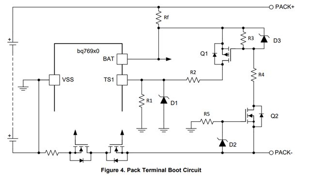
We are designing 4S BMS using BQ76920 and facing challenge to design wake circuit for BQ. As we were considering multiple options for wake-up circuit and came across  http://www.ti.com/lit/pdf/slua769.

Can anyone explain in detail how the circuit works as show in figure 4 of the document.

  • Hello Samarth,

    When the charger is placed across the PACK terminals, Q2 will turn on as long as the charger voltage is at least greater than the Vgs threshold for Q2. This is because PACK- is not referenced to Vss at this point, so the source voltage of Q2 becomes Vbat - Vcharger.

    The gate of Q2 is referenced to Vss, so when Vbat - Vcharger (the source voltage) < Vthreshold, the gate-source voltage becomes 0 - (-Vthershold) = +Vthreshold. This enables the Q1 FET by drawing current through R3 and R4. So D1 is placed in order to protect the TS1 pin from overvoltage due to the PACK+ voltage. 

    D3/D2 protect the Q1/Q2 FETs respectively if needed.

    When the system boots up PACK- will be referenced to Vss, so the Vgs of Q2 goes away and the Q2/Q1 FETs turn off, allowing TS1 to return to a normal voltage.

    This is all explained in page 4 and 5 of the bq769x0 boot switch alternatives application report that you linked.

    Best Regards,

    Luis Hernandez Salomon

  • Hi Luis,

    Understood, thanks for quick response!