This thread has been locked.

If you have a related question, please click the "Ask a related question" button in the top right corner. The newly created question will be automatically linked to this question.

TPS43060: Inconsistent start-up issues with the boost IC and Low Side MOSFET

Part Number: TPS43060


Hi TI Team,

We are using TPS43060 in our design with following specs:

Vin 10.8V - 15V
Vout 24V
Iout 2A
Fsw 400kHz

The design does not look incorrect but there are following observations:

1. Board #1: We concluded that the boost IC is damaged due to following impedance checks

HDRV to gnd 3.3Ohm
LDRV to gnd 0.5Ohm
Vcc to gnd 1.8Ohm
Boot to gnd 1.8Ohm

2. Board #2: The drain and source of the low side MOSFET appeared to be short. Initially the board boosted output voltage to Vin+3V but eventually failed.

Both the boards were not subjected to any loading conditions when they were damaged. It was initial programing of the boards with EN being pulled high by the microcontroller.
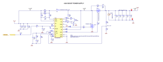
Schematic snippet

Let me know your thoughts on the design.

  • Hi Ashwini,

    Thank you for designing with the TPS43060.  There are 4.7 Ohm gate resistor which may reduce the dead time between the high side and low side MOSFETs.  Could you please monitor the two MOSFET's Vgs voltage waveforms and see if there is enough dead time?  

    Thanks,

    Youhao

  • Hi Youhao,

    Please find the waveforms there are issues that we can see. Dead band is definitely less which is a major concern but there is a 6.6V drop in HDRV waveform which is not understandable.

    We could not get anything out of damaged boards but the waveforms on working boards are also not fine. Please find the waveforms below from a working board

    Loading conditions: Vin = 15V, Iout = 0.5A from a DC Electronic load in CC Mode

    HDRV Vs VCC

    HDRV Vs LDRV at MOSFETS pin

    Deadband Issue

    HDRV Rise Deadband which is fine

  • Hi Ashwini,

    I would recommend decreasing the impedances of the low and high-side FET in order to force a faster turn-on/off. As for the 6V drop, I believe what you are seeing in the first waveform is after the high-side MOSFET conducts, the boot-strap capacitor is mostly discharged, so the voltage across it is small. Therefore, the high-side gate voltage just sees the voltage across the boot-strap capacitor and SW pin, which is at 24V. You can check this by probing the difference between HDRV-SW, alongside with LO to check for the actual dead-time.

    A question I have is that you mentioned the IC is damaged during EN turning on. How high are you pulling up this pin?

    Regards,

    Richard

  • Hi Richard,

    1. By decreasing the impedance, I believe you mean decreasing the total gate charge (Qg) and gate resistor of both the MOSFET. Is that correct?

    2. So is the waveform I am seeing on HDRV a valid waveform or do I need to increase the value of bootstrap capacitor to hold the charge for a while longer?

    3. The EN pin is maximum 3V3 as it is driven by a microcontroller

  • Hi Richard,

    Please find the waveforms below. The deadband looks about 60ns which is good enough. Definitely not the cause of failure

    Yellow: SW

    Green: HDRV

    Blue: Math C1 - C2

    Orange: LDRV

  • Hi Ashwini,

    1) I just meant the gate resistor of the MOSFET.

    2) Thanks for providing the waveform below. For future reference, when checking the dead-time it is important to check LDRV, and HDRV-SW to get the actual waveform to check the dead-time.

    3)  Your EN condition seems correct here, so can you replicate the failure on a working board using an ABA test? 

    Regards,

    Richard

  • 1. The dead time recorded in the waveform HDRV-SW and LDRV is 58ns - 60ns which is ok. Deadband doesnt seem to be the problem as per the waveforms attached earlier. Do we still need to reduce the gate resistor? It increases the ringing

    2. The ABA test the boards failed at B

    Board #1: All short in VCC, HDRV and LDRV

    The IC was changed. There is no short now but there is no internal VCC of the IC generated

    Board#2: Eventual failure of the low side MOSFET

    The low side MOSFET was changed but there was no VCC of the IC. Then the IC was changed. Now we can see the internal VCC of the IC but it still stands disabled. The IC doesnt drive any of the MOS

    Will look more into those board this week.

  • Hi Haroon,

    Thanks for providing the information. When you say there is no internal VCC, are you saying that the VCC pin reads 0V?

    Regards,

    Richard 

  • Yes it reads a flat 0V but there is no short with the gnd 

  • Hi Ashwini,

    Can you check the continuity of the VCC pin to the VIN pin and the BOOT pin? It seems strange that you could see VCC on the board and now it is not apparent. It makes me think that this is a connection issue. 

    Regards,

    Richard