This thread has been locked.

If you have a related question, please click the "Ask a related question" button in the top right corner. The newly created question will be automatically linked to this question.

LM51561H: LM5156 not stable at high power

Part Number: LM51561H
Other Parts Discussed in Thread: LM5156H, , LM51561, LM5156

My boost design is the following :
Input = 5V-14A
Output = 9V-3A max or 12V-3A max or 15V-3A max or 20V-3A max, for USBC source application
I select the wanted output voltage by changing the feedback resistor Rfbb.
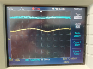
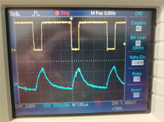
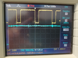
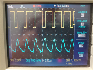
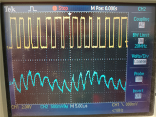
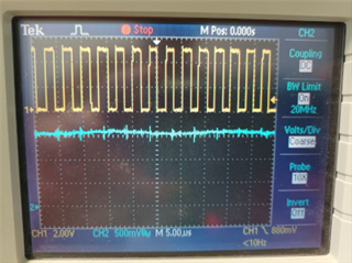
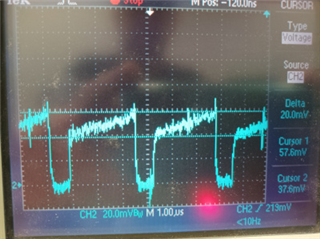
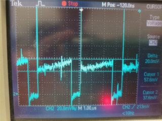
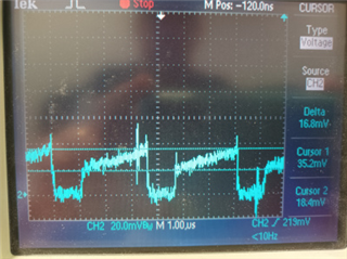
All voltages works well with a light load (~1Kohm).
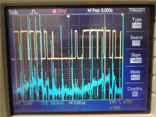
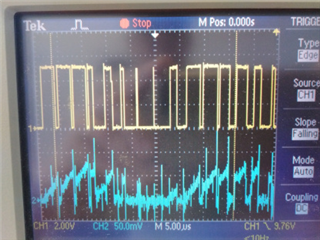
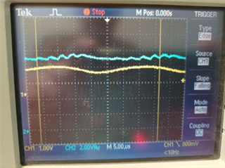
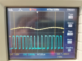
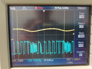
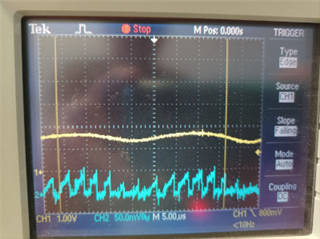
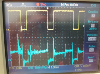
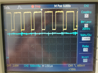
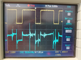
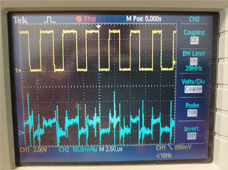
I've tested 9V, it works until 14W, but is not stable after (around 18W). Not stable means that the voltage tries to go to 9V, but decreases to ~5V (chip is Off, I suppose), and retries every 125ms.
I suppose it is the Hiccup Mode Overload which occurs, because on my prototypes, I used LM51561H instead of LM5156H, for availability reasons.
For 15V, it doesn't work @ 12W.
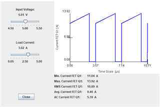
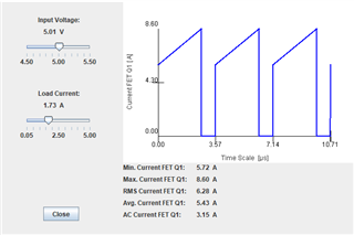
I did several simulations on webench, and selected the worst case values of each component, and make validate my design with FAE in France, but it doens't work.
Can you check my design, and tell me what component should be changed ?
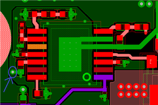
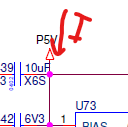
Here are the schematics :

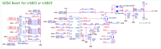
Here are the main components BOM :
U73 = LM51561HPWPR, Q49 = SQJ152ELP, D102 = SDT20B100D1-13, L42 = PA4343.472ANLT

All is OK on my board, this is the last stage to make work, can you help me quicly please ?

Thank You.

  • Hi Olivier,

    Based on your description it looks like the devices detects an overcurrent on the CS pin (current sense input) as you already assumed.

    Can you probe the input on that pin with a scope (please use a very short ground loop - tip barrel method to avoid pick up of noise).

    When measuring the SS pin you should in this case also see a ramp up and discharge which will indicate the overcurrent detection as well.

    I assume that RFU means not assembled but maybe you can confirm.

    Best regards,

     Stefan

  • Hi Olivier,

    there is another thread where this issue is discussed already, so as suggested in the other thread i will close this one.

    If you would like to reopen it again, just add another reply and it will open again.

    Best regards,

     Stefan

  • I follow in this thread.

    Here is a screenshot of gate/RS:

    As I begin to understand how it works, it seems that duty cycle isn't stable, and is too high, so current sense limit is overflowed. Could it be a layout problem, or any filtering not enough ?

    Regards.

  • The last screen was with Rs=6.67ohm.

  • Hi David,

    now that the over current is not triggered anymore we can see that the duty cycle is not stable.

    See that short and long pulses on the Gate.

    This indicates that the slope compensation is not high enough. 

    So for the 6.67 mOhm sense resistor can you please try to  replace R508 with ~ 700 Ohm.

    When going back to the 10mOhm it should be in the range of 1.7kOhm

    See also datasheet section: 9.3.7 Current Sense and Slope Compensation (CS Pin)

    Best regards,

     Stefan

  • OK, I will try this afternoon.

    I read at least 20 times the section 9.3.7, but I obtain differences between webench results, your excelsheet calculations and my own calculations based on your datasheet, and I can't find where are the errors.

    So can you retune my design values, especially Rs, Rf, Cf, Rsl, and tell me the precise calculations to follow to obtain it :

    Vin_min = 4.88V

    Vin_max = 5.49V

    Iin_max ~ 13A.

    I have 4 usbc voltages to manage, each output voltage can feed 3A max. I have to find a BOM to cover all the 4 voltages. According to Rfbb precision 1%, I tell you the output voltage min and max :

    Vout = 9V : 8.94V to 9.45V, 9.19V typ., 3A max

    Vout = 12V : 11.90V to 12.60V, 12.25V typ., 3A max

    Vout = 15V : 14.87V to 15.75V, 15.30V typ., 3A max

    Vout = 20V : 19.82V to 21.00V, 20.40V typ., 3A max

    Thank you.

  • I've replaced R508 by a 820 ohms, and it's not really better... Probed P21G and CS pin directly:

  • Hi Olivier,

    the signal on the CS pin is really very noisy - may you can try to enable the bandwidth filter on the scope for this channel.

    Nevertheless if the Slope compensation does not improve the heavy jitter on the switch node signal, some other problem needs to be in the system.

    Maybe you can share the layout, iI really would like to ensure that this is not related to something in the layout.

    Best regards,

     Stefan

  • Would increasing Rf/Cf to improve the noise be a good idea ?

    I send you my layout, but I send it to you through French FAE, as it is higly confidential.

  • Hi Olivier,

    thank your for the layout, will send the information back via the FAE once i received and reviewed it.

    Increasing the filter might not help, esp. when not understanding where the disturbance is coming from. Making the filter to slow does also delay the current information for the LM51561 and therefore influence the full regulation loop.


    Best regards,

     Stefan

  • Hi Olivier,

    i have reviewed the layout but need seen a major issue.

    I also took one of our EVMs and modified it to meet your setup.

    Using this conditions: 

    Vin = 5V   Vout = 12V   /  I load = 3A

    Inductor = 4.7 uH    Rsense = 5mOhm

    Ch1: Switch node  (P21D)

    Ch2: Comp

    Ch3: Voltage at Current sense (R505)

    Ch4: inductor current.

    Even without bandwidth filtering i get very clean signal measured.

    Have you used a very short ground loop - tip barrel method to avoid pick up of noise?

    Can you also check the waveform on the comp pin?

    Thanks,

     Stefan

  • Hi Stefan, as i'm not an analog expert, it's possible that my layout is not clean enough. Can you check it, and tell me where would be the error, and if I can test an improvement by adding a wire, to verify that a layout modification would fix the problem.

    Thank You.

    Regards.

    Olivier.

  • I will add the comp pin to show you, and check which design rule could be not followed.

    After the layout verification, could you advice me about what values should be used on my design, because I always don't know what should I use as Rs, Rsl, Rf, Cf.

  • I had a look at my layout, and I think I found where the problem is, can you confirm me :

    I have put in blue on the bottom-left of the layout, there is a VIA which connects the local analog ground which is in L8 (bottom) and L7 to the digital GND. This via shouldn't exists here.

    Could it be the problem ? If you think yes, I will try to remove it (very delicate operation).

  • Hi Olivier,

    you are right this really can trigger the issues esp. as next to this the great GND connection. This means a lot of current the be flowing in the ground plane and disturbing this node/via. I definitely would give it a try.

    Once we have the system basically stable then let us try to tune the system for better stability with the Rs, Rsl, Rf, Cf.

    A first point for having 20V / 3A output the sense resistor should be 5.57mOhm or less.

    The other parameters can then be more easily optimized.

    Best regards,

     Stefan

  • Hi Stefan, good news, it works now, output power is stable !

    My layout sub-contractor will hear about me...

    So now, is it possible for you to confirm me the values you think for all the parts around ?

    I will continue to raise the output power, but I would prefer to put the final values you compute.

    Regards.

  • Sorry, in fact, I've made a bad test, my load was not correctly connected...

    For the moment, it's the same, I will check if my hole is good enough, but difficult to be sure.

  • Hi Stephan,

    After having verified that my local GND was really isolated, nothing is better, so go back to the starting point.

    I'm desesperated to pass 2 weeks on such a simple chip, without finding the solution, it is the last part of my board to validate, and I'm very hurry.

    I took new screenshots, can you really check my layout, check my values, and give me steps to find the issue ?

    As my design is very little, I've took different screenshots separately, with COMP pin as the common signal CH1 between each, and CH2 with BW limited.

    Conditions : Vout~9V, R_load~12 ohms, R505=5mohm, R509=820ohm, the rest hasn't changed.

    CH2=Vin (P5V) => 200mV peak-to-peak for input voltage ripple.

    CH2 = Vout (P_SRC) => ~600mV peak-to-peak for output voltage ripple.

    CH2 = Gate (P21G)

    CH2 = P21D

    CH2 = CS at pin 7

    I hope you'll find the problem very quickly.

    Best regards.

    Olivier.

  • Hi Olivier,

    with this setup you have almost no phase margin.

    Can you replace 

    R558 : 1.7kOhm

    C445: 68nF

    and probe again. (output ripple should be in the range of 20mV)

    If this would be OK the test with Vout= 12 and Vout=20V

    Best regards,

     Stefan

  • OK, now it works (at least!).

    I put 1.78K + 68nF. (I don't have 1.7K)

    Output ripple is smaller, but still too high : 320mV for 9V on 12 ohm, and 500mV for 9V on 6.8ohm.

    Perhaps should we resolve that before going on higher voltages ?

  • Sorry wrong button

  • I tried 15V-12ohm, ripple~700mV, 20V-12ohm gives ripple around 1.2V

  • Hi Olivier,

    i checked the components of your design against the loop stability and come up with this values:

    R505 : 5 mOhm   (R Sense)

    R508 : 0 Ohm      (R Slope)

    R509: 100 Ohm

    C444: 1nF

    Compensation:

    R558: 2k Ohm

    C445: 100n

    C460: 1n

    This seems to give enough stability for the output voltages from 9-20V.

    Best regards,

     Stefan

  • By C558=100n, you mean C445 ?

  • And should I keep R509=820 ohm or I come back to 100 ?

  • Hi Olivier,

    just updated the message above.

    Best regards,

     Stefan

  • Hi Stephan, these values don't improve output ripple.

    I did a test at 20V-6.8ohm, so should be around the maximum power 60W, and 20V is not totally stable. This must be another issue.

    What can I do to find the output ripple problem ?

  • Hi Olivier,

    how did the general behavior change now?

    - Is it stable at 12V

    - How does the Gate signal now look?

    - How is the Comp pin?

    Best regards,

     Stefan

  • General behavior seems good now.

    At 15V, 6.8ohm, COMP is flat, CS is rectangle, GATE duty cycle is stable, but output ripple is 1.2V.

  • Hi Olivier,

    thanks - great to see that we are on the right track now.

    Can you please share a few scope pictures:

    Output ripple with:

    - gate

    - Comp

    - CS

    Can you also let me know the output ripple at other voltage (e.g. 9V, 12V, 20V)

    Thanks,

     Stefan

  • Here are the new measurments. CH1 = GATE on each plot.

    20V-12ohm (6.8ohm doesn't work):

    CH2=Vout in AC:

    CH2=COMP

    CH2=CS

    15V-6.8ohm:

    CH2=Vout in AC:

    CH2=COMP:

    CH2=CS:

    9V-3.5ohm:

    CH2=Vout in AC:

    CH2=COMP:

    CH2=CS:

  • Hi Olivier,

    can you try to replace the 100uF with 50uF - the AC current of 5.6 A is quite high for an capacitor.
    (you can also take 2 x 100uF if you have then available)

    Can you please also share the part number of the used capacitor - if this is a MLCC i would like to check the DC bias.

    With 9V: the first picture shows a not stable gate clock, while the others are OK. Can you check this again?

    Best regards,

     Stefan

  • C441 is a chimik SMT, 865080545012 from WURTH. C440 is a MLCC standard ceramic 10uF 10% 35V X6S CR0805.

    I suppose the problem comes from C441. If yes, can you tell me the specifications to follow for that ?

    For 9V, it is stable if I draw less output current, but when I approach to the maximum current, it is worse. 20V-3A is not stable at all.

  • Hi Olivier,

    the 865080545012  is a Aluminium Electrolytic Capacitors with a relative high ESR of ~ 370mOhm.

    With a Capacitor RMS current of ~5.6A  (@ 20V/3A output) this give the seen voltage drop/voltage ripple on the output.

    (Where the 10uF compensate the higher peak)

    Please try to use an output cap with lower ESR e.g. 875115652007

    But as you have a quite high RMS current for this capacitor I recommend to replace this by 2 or 3 capacitors in parallel to split the ripple current to several capacitors, otherwise it might be overheated.

    Best regards,

     Stefan

  • OK thank you.

    Seeing the price of such capacitors, I think I will use ceramic capacitors only. Do you think I can stay with 25V capacitors ?

    Now ripple is explained, we have to find why 9V-3A isn't enough stable, and 20V-3A doesn't work at all. Can you explain me your calculations for phase margin ? I suppose it comes again from that, no ?

  • HI Olivier,

    of course you can use ceramic caps but keep the DC bias degradation in mind, so the effective capacity of MCLL is lower when used in DC.

    25V caps is very low margin, typically the margin for the voltage used for the output cap is ~ 40-50%  (under more critical applications even 100%).

    This ensures the capacity is available even under high temperature and aging conditions.

    I am not sure if I understood the second question right. For evaluation of the loop response you can use the 

    LM5155/56 Flyback Controller Quick Start Calculator

    The mathematic is described here as well:

    How to Design a Boost Converter Using the LM5156

    Best regards,

     Stefan

  • OK, I see.

    Now, can you help me to find the good values to make 9V-3A stable, until the 20V-3A ?

  • Hi Olivier,

    once the output capacitor is defined the loop stabilization can be evaluated. (The parameter of the output capacitor needs to be known as it impacts the loop compensation)

    For this you can use the quickstart calculator (see above).

    You need to test on the different conditions you have for input and output voltage to find a suitable setting for this.

    Best regards,

     Stefan

  • Hi Stefan. I've tested polymer capacitor, 100uF-0.031ohm. Ripple was still high, for 9V-3A, 680mVpp. I tried to put an other 100uF in parallel, and gives 380mVpp. I tried to replace the polymer with 5x22uF ceramic, and here it was very better, 160mVpp. But with 20V-3A (which works well now), I have 1.62Vpp ripple, so still bad.

    I can't find anywhere a formula to estimate the output ripple, can you give me one ? It is for me to know the influence of ESR on the ripple. Is there any way to unlock the excel, for me to see on which formulas ESR has an influence ?

    As I don't have enough place to put a too big capacitor, I was thinking to put 11x10uF ceramic capacitors at the output, but I'm still not sure it would be enough for 20V. Do you have any advice ?

    With excel calculator, I tried to evaluate the loop compensation. Can you tell me what is an acceptable phase margin ? Is it right that I have to keep crossover frequency under the maximum value the excel is calculating in "suggested maximum bandwidth" ? If it is that, I'm not sure to find a tuning which works well at the 4 output voltages. Can you help me for that ? My final values for voltages and resistor used will be : RFBT=20K, RFBB=2441.6 for 9.19V, RFBB=1778.4 for 12.25V, RFBB=1395.5 for 15.3V and RFBB=1030.8 for 20.4V.

    Last remark: on my board, it was not a layout problem, as the board with the layout corrected and a board without reacts the same, so it is just the values which are wrong.

  • HI Olivier,

    there is application report which describes all the calculation:

    How to Design a Boost Converter Using the LM5156 (ti.com)

    Chapter 3.7 shows the calculation for the output capacitor.

    More details on the ESR of the output capacitor can be found in:

    Topic_3_Lynch.pdf (ti.com) (page3-15)

    Phase margin and compensation limits are very good described here:

    Switch-mode power converter compensatin made easy   (Page 4)

    As you can see from this document the power stage need to be defined first (including the output capacitor).

    The bandwidth can also be sligthly higher - but there should be a high enough distance to the switching frequency and the RHPZ.

    When testing the output ripple, please check if the ripple is related:

    - to the switching cycle and indicates that either the output cap is to low or the ESR is to high. (Ripple frequency is switching frequency)

    - to instability of the output and compensation loop, where the ripple frequency is typically lower then the switching frequency

    Best regards,

     Stefan

  • Hi Stefan,

    On behalf of Olivier:

    Sorry for my last post, I did a mistake, because I’m very busy and hurry, and I’m tired to pass 3 weeks to tune a DCDC…

    I did new measurements on my board which have the 10uF ceramic + 5x22uF ceramic. Rload is always stable, as I use power resistors.

    9V-3A: OK, ripple is ~160mV @ 290KHz

    15V-3A: OK too, ripple is ~300mVpp @ 290KHz

    20V-3A: doesn’t work in fact, I’m back to the first problem, it begins to work and that cuts.

    20V-2.4A: doesn’t work neither

    20V-1.65A: OK, ripple is ~270mVpp @ 290Khz. D~75%, comp is flat (see image).


    It seems I can’t go over ~45W.

    To remind,iIt is with the values you gave me:

    R505 : 5 mOhm   (R Sense)

    R508 : 0 Ohm      (R Slope)

    R509: 100 Ohm

    C444: 1nF

    Compensation:

    R558: 2k Ohm

    C445: 100n

    Regards,

  • Hi Sebastien, 

    can you also attach the image with is mentioned above.

    Best regards,

     Stefan

  • Sorry....

    Here it is:

  • Hi,

    From the description above i would assume this picture should show : 

    "comp is flat (see image)" 

    with Vin 5V/ Vout 20V /1.65A ?

    For me this looks like the signal on CS.

    Best regards,

     Stefan

  • When assuming this is the voltage on the current sense pin this would exactly match to a load current of 3A with Vin 5V and Vout 20V

    Best regards,

     Stefan

  • Hi Stefan,

    OK, the forum works again for me.

    Yes, it was the pin1, and I've just verify it again, Vin is still 5V, and Vout is 20V (20.6V), the load is 12 ohms, it can't be 3A load current (it is a true power resistor, I've checked it's value). Rs is 5mohm-1W, I've changed it to have a true 5mohm.

    Where is the problem ?

  • Hi David,

    yes, the forum was down for a few minutes, I had the same issue.

    Can you help me to understand - which pin 1 - pin 1 on LM5156 is BIAS.

    I am really confused on the currents if the waveform is on CS: do you have a chance to measure the input current for this power stage. (Measurement with a multimeter would be OK. 

    20.6V^2 / 12 Ohm => P out 35.36 W  -> 90% efficiency P in = 38.9 W  -> I_in (5V) = 7.78 A

    As mentioned the waveform looks like the current for 3 A output

    with 5mOhm this is

    V(cs - max) = 70mV

    V(cs - min) = 55mV

    With 12Ohm load -> 1.72A this would give:

    with 5mOhm this is

    V(cs - max) = 43mV

    V(cs - min) = 29mV

    Note: this pictures are made with Power Stage designer.

    Best regards,

     Stefan

  • Yes, sorry, it is pin 7, CS.

    I won't be able to measure Input current on my board, too difficult. Could I do any other indirect measures ?

  • I have verified the voltage on R505, it is the same as pin 7 :

    If I change output voltage to 15V, on the same 12ohm load, it does like that:

  • Hi Olivier,

    can you make a delta measurement of the supply current of the complete application with EN_PRSC1  (Enable on LM5156).

    Maybe you can control this signal.

    The delta in the current should then show the calculated value.

    Best regards,

     Stefan