This thread has been locked.

If you have a related question, please click the "Ask a related question" button in the top right corner. The newly created question will be automatically linked to this question.

TPS5450 PCB layout question

Other Parts Discussed in Thread: TPS5450

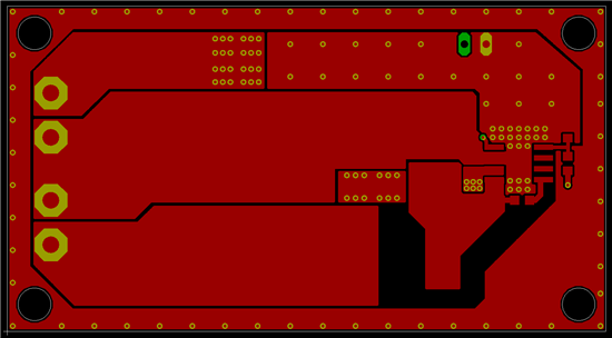
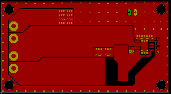
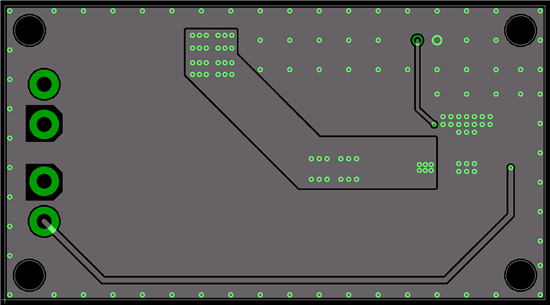
I noticed that the TPS5450 EVM PCB pretty well keeps all the ground current flow on the top layer by keeping the ground planes for layers 2-4 away from the Vin and Vout GND pads and only stitching the ground planes together at the TPS5450's thermal vias, the EN jumper header and TP4. It seems that the GND planes for layers 2-4 are only for heat dissipation and not for lowering GND impedance, helping to reduce emissions, etc.

I'm laying out a board using the EVM's design as a starting point and was wondering what the advantages and disadvantages might be if I "stitched" together the ground planes with vias and also allowed the GND planes to connect to Vin/Vout GND pads? It would certainly lower the GND plane impedance (possibly helping to reduce emissions and increase immunity?) but could that cause problems?

I was also considering enlarging the top layer GND plane and having it essentially encircle the Vout power plane and the components.

Thanks!

  • There are different techniques you can use for grounding, but basically, there are two main approaches as you have noted.  You can force the current flow by isolating traces and fill areas then connecting them together at one place "star ground" or tightly coupling all ground areas with multiple Vias.  there are proponents of each.  Star ground works particularly well when constructing boards that contain only a single circuit such as this EVM.  For specific PCBs that contain multiple circuit elements, the distributed ground is more effective.  Make sure to use plenty of vias at the critical return locations (ground side of the input and output capacitors).

    All that being said, the TPS5450 is right at the limit of power dissipation in that 8 pin DDA package.  At 5 A output the junction temperature rise is near 100 C. on the EVM.  For most applications.  More copper will be required.  We have a copper area estimator tool, but the TPS5450 is not yet supported.

  • That copper area tool would have been handy. :-) If it allows for a generic heat source of a specified size, I could just use the power-dissipated number for the TPS5450 and experiment from there.

    Thanks for your input on this!  The TPD5450 circuit will be just one of 5 circuits sharing the same PCB (including 2 other switcher circuits and a microprocessor). I ended up leaving the top layer GND copper (for the in/out caps and diode) isolated from the rest of the ground copper except at the TPD5450's GND pin. I also left the input and output GND connection points isolated from the other layers too (as is done in the EVM).

    But, I expanded the copper from the underside of the TPS5450 a lot and realized that since that top copper would be so well tied to the other copper layers because of the thermal vias, I could connect it to the rest of the top copper layer. The image below shows the PowerPad copper expanded but not connected to the GND copper I have around the outside of the board.


    This next image shows the PowerPad copper joined to the other top layer GND copper. Ignore the number of vias I have for now.


    I kind of like the idea of keeping the heavier switching current flow in the top layer central GND plane, isolated from all the other GND layers except at the GND pn and PowerPad connection point. Don't know if this is a good idea or not though. :-)

    A small board run is being done to test the circuit in several prototypes along with the other circuits. Eventually, the TPS5450 circuit would be lifted almost as-is and dropped onto the larger board. The peripheral GND vias would not be so numerous and GND would be delivered to this circuit via a bunch of vias to the other GND layers replacing the two GND center connection points on the left. This, I thought, would keep the heavier switching currents on the top layer, isolated and away from the main GND layers, but still allow for low-impedance flow between the TPS5450 circuit's components.

    At least, that's the idea. If you feel this approach might be a problem, please let me know. A couple more images to explain the circuit follow below. The circuit is laid out follwoing the EVM as an example. C7 and C8 in the upper left are bulk caps since the power is located up to several inches away from the board. D2 is a TVS diode for some ESD protection as the prototype output connections will be handled a lot. I'll be swapping positions of D2 and C10.


    The image below is layer 3. The other two layers are solid GND copper but leaving the two GND connections isolated as is also done on this layer..


  • Hi John, looks nice!

    I was just wondering why you didn't use tantalum capacitors. I'm trying to fit the TPS5450 in 0,8" x 1,4" of two layer board space.

    Therefore tantalum caps could help keep it small.

    Would be nice if you could shortly report if the design worked well...


    Thanks,

    Bob

  • Hello Bob,

    Thanks! The board works perfectly but at 5A (continuous), the case temperature of the TPS5450 is about 102C. And this is with a 4-layer, 1.4" x 2.4" board in open air, with lots of thermal vias...darn hot. :-)

    For production, I have about 4x more copper area available and a bit of active air flow to help with cooling so I'm not concerned. If you're running over about 3A continuous though, I'd recommend going to a larger board size and using 4-layers of copper to help spread the heat. Or active cooling. I guess testing is the only way to know for sure though.

    I didn't use tant. caps for cost reasons. I have enough space for the (low-ESR) electrolytics so their size wasn't a problem.


  • Hi John,

    thanks for the feedback and the advice on temperature.

    I won't need much more than 2,5A, but hey, i like having some reserve, who knows what will come...


  • Sounds like you'll be OK with that board size then...I think. :-)

    Let us know how the board works out!

  • Well, has been a while, was busy with other stuff too.., but after all it works not that bad!

    IC stays "cold" during operation, and i could even switch to 470µF aluminium caps after pushing around some other components and getting a liitle bit more space.

    But i don't like the ripple on the input voltage, it's around +-300mV and i really would like to see way less of that!Seems like i have to squeeze my brains over this now...

    Output is fair enough with +-70mV, but could be better.

    Below is my attempt on a design for this nice little device:

  • Nice!

    Just as a reference, here are the numbers for my board and some test results:

    • Tested at 19.0V in, 13.8V out.
    • 50C. max PCB temp. after 1 hour "soak" at 2.8A.
    • 40C. max PCB temp. after 1 hour "soak" at 2.0A.
    • +160/-90mV peak input ripple at board's input solder pads, at end of 30" of cable from switcher supply. Most of the ripple is from this supply.
    • +/-15mV output ripple at output solder pads, 6" twisted leads to resistive load.
    • Twin 82uF polymer elect. caps on output.
    • Twin 100uF elect. and twin 4.7uF MLCC on input (plus 0.01uF MLCC at chip).

    I agree, seems you should be getting lower ripple readings. Depending on your cap., and supply of course. Bump up your inductor value a bit?

    I seem to be running hotter than you though. Was your board staying at essentially room temp at 2.5A? I'm wondering if perhaps my soldering of the GND pad isn't perfect. I don't have thermal vias underneath the chip (to ease manufacture) but that shouldn't make much more than a few degree difference IMHO. Certainly not the difference I'm seeing between your board and mine.

    I do have lots of 15mil (drill) vias nearby the GND pad though. My switching to 10mill (drill) vias and increasing the quantity would help a bit, but probably not by much.

    [Edit] Hmm...your layout is in the copy of your post I received by e-mail but it's not in your post here.

  • "cold" might have been the wrong term, it's not running hot as hell... Allthough i haven't measured, i'd guess around 35°C-40°C with 2A load.

    Since i've seen diodes unsoldering themselves, everything <60°C is "cold" ;-)


    I'm also wondering where the image is... i can't see it neithere on the site, nor in the email i received... strange!


  • Ahhh...OK. Sounds like we're running at about the same temps.

    I was mistaken about my input ripple though. I neglected to check the ripple frequency...it's 500kHz. Almost none is from the switcher supplying power to the board, it's from the TPS5450. For my application it's not worth adding more cap. to reduce it further though.