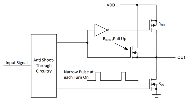
TI’s Gate Drivers specify both pullup and pulldown resistances of their output stage. Many of TI’s Gate Drivers have a unique output architecture on the pullup structure, which delivers the highest peak source current when it is needed most, during the AC transition from low to high (Miller plateau region). The device output stage features a hybrid pullup structure using a parallel arrangement of N-Channel and P-Channel MOSFET devices. By turning on the N-Channel MOSFET during a narrow instant when the output changes state from low to high, the gate driver device is able to deliver a brief boost in the peak sourcing current enabling fast turn-on. This hybrid structure is show below in Figure 1:

Figure 1: TI’s Hybrid Output Structure
Using TI’s new dual channel low-side gate driver as an example, the UCC27624, its hybrid pullup structure’s N-channel MOSFET (RNMOS) has an on-resistance of approximately 1.04 Ω when activated.
Those with a keen eye will notice the pullup resistance specified in the datasheet table below (from the UCC27624 datasheet) is significantly higher than the 1.04 Ω of the NMOS MOSFET alone. This is because the data in the table is taken as a DC measurement rather than an AC measurement, and it is representative of the on-resistance of the P-Channel device only. The NMOS MOSFET is only on during the AC transition from low to high. The AC pullup resistance is further explained in the “Output Stage” section of UCC27624’s datasheet.

The pulldown structure in the UCC27624 device is simply comprised of a N-Channel MOSFET. Therefore, the ROL parameter, which is also a DC measurement, is representative of the impedance of the pull-down stage in the device. Additionally, if the part features a PMOS only pull-up structure, then the DC ROH parameter would be representative.
If the TI device does not explicitly state the effective AC resistance of the hybrid pull-up structure, it can be estimated to be approximately 1.5 x ROL.

