This thread has been locked.

If you have a related question, please click the "Ask a related question" button in the top right corner. The newly created question will be automatically linked to this question.

LM5060-Q1: LM5060-Q1

Part Number: LM5060-Q1
Other Parts Discussed in Thread: LM5060

Hello

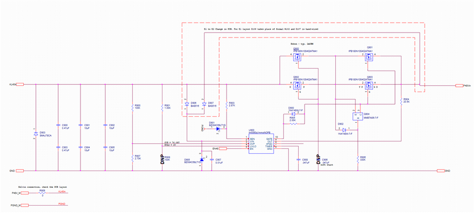
i have used the LM5060 circuit braker layout from TIDA001168 design two issues:

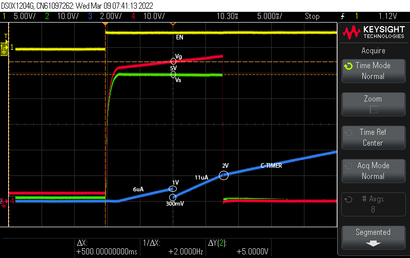
1) When i use C-TIMER capacitor 0.047uf. after EN goes high, the CAP does the 6uA ramp, Vgs reaches 5V and the CAP discharges to 300mV. then it starts to charge at 11uA and it reaches 2V and Vgs gets shut down.

 - i have looked at all the setups and components. all is as it is in TIDA001168. please see sch attached.

 - Output KL40 is isolated and not connected to any power source or load.

 - output ramps up and after VGS shutdown, output ramps down and this keeps repeating.

2) i have removed the C-TIMER and grounded the TIMER pin. this works fine. the MOSFET turn on and off and i can EN and DISABLE them. ( obviosly i dont have all the protection this circuit offers)

3) With TIMER to GND.

  - I connect two of these board in parallel. the P48V comes from different supply sources.

  - KL40 is common and connected to the external 50V source.

Not load and no Supply at the KL40 pis

  - i cannot start them MOSFETS when i apply EN to the LM5060

  - P48V has 49V on it. KL40 remains 0V

With KL40 = 49V

  - the circuit works and i can turn the breakers ON and OFF.

need your insight.

thanks

  • Hi Shahram,

    Thanks for reaching out!

    Can you please share the test setup, test conditions and test waveforms for each of the case to look into the issue.

    Best regards, Rakesh

  • Hi

    please see the waves for # 1 above

  • Hi Shahram,

    It looks like a Vds fault (similar to Figure 23 in data sheet). What is the load here?

    Best regards, Rakesh

  • Hi Rakesh

    The output (KL40 side) is not connected. it is unloaded, other than the CAPs and diode and resistor dividers setting up UVLO and OVP limits...

    i measures the OUT and SEN pins SEN > OUT by about 350mV

    Regards

  • One more note

    the KL40 to GND side is ~23KOHM

  • Hi Rakesh

    it seems to be the Rsense and Rout that are not correct and cause the fault.

    i have calculated and tried various values and i don't seem to make it right.

    1) used the TIDA001168 values. Rs = 2.87K and Ro = 20.5K. we see the behavior I explained earlier.

    2) varied the Ro numbers around 1K to 15K and the FETs start but when i take enable away. The out does not shutoff all the way. from 49V goes down to 42V... but not to 0V. it seems the MOSFET becomes the carrier through the LM5060 and heats up.

    Can you please suggest Rs and Ro values based on the sch above and these parameters

    - KL40-GND are connected to the outside world. Voltage will be 40-65VDC.

    -P48V-GND is internal to our design and will float between 46V-51VDC. we have very accurate control on this. CV source and regulated current. 10A max on the 50V coming in to P48V.

    Thanks

  • Hi Shahram,

    Thanks for the details. For the second case, have you measured GATE to source voltage ?

    Can you please try below changes and let me know if it helps.

    1. Rs = 2.87K and Ro = 1K  {we need to use equation 21 in the data sheet to set the circuit breaker current threshold}

    2. Connect Ro to the common source point as shown below. {Ro connection at the output which is active bus can leak currents into the gate}

    Best regards, Rakesh

  • Hi Rakesh

    I have not measure that... will do

    i have tried 1. Rs2.87K and Ro1K. the MOSFETS turn on and all looks good. BUT, when i disable EN. voltage gors from 49V on KL40 down to 44V. i tired pulling 2A of current through, thinking the cap had held the voltage up. but the FETs where not completely off and kept supplying power at 44V and the MOSFET got hot.

    Will try 2. later today thanks.

    what values should i use... Rs2.87K and Ro? 1K or 20.5K?

    thank you

  • Use Rs=2.87K and Ro=1K

  • OK i moved Ro to the inside of Q903 as you suggested. didn't do much.

    then i moved Rs to the P48V side of Q903. didn't do much, MOSFETs were shut down, no gate activity.

    then i realized UVLO was not high, because power will always start from them P48V side. so i moved that over to that side as well.

    All is good now. it is working properly

    Do you see any issues with Ro and Rs being where they are now ?

    Thanks for you support

  • Keeping Ro to the inside of Q903 is better option for system with active bus at Vout. This avoids leaking any current in to the GATE.

    Best Regards, Rakesh