Because of the Thanksgiving holiday in the U.S., TI E2E™ design support forum responses may be delayed from November 25 through December 2. Thank you for your patience.

This thread has been locked.

If you have a related question, please click the "Ask a related question" button in the top right corner. The newly created question will be automatically linked to this question.

LM27402: How much current can VIN pin handle

Part Number: LM27402
Other Parts Discussed in Thread: , TINA-TI, TPS24771

Hey TI team,

I am using LM27402 for a 5V 20A circuit. I wanted to know what is the significance of Rin and how its value is decided?

How much input current can the Vin pin handle?

When the input source is a high current low voltage source, what should be the value of the input capacitor be?

How to avoid high inrush current in the IC at startup?

  • Welcome Back,

    The RIN is part of the filter.   The RIN value is discussed in LM27402SQEVAL user guide section 9.1. 

     https://www.ti.com/lit/ug/snva406c/snva406c.pdf

    use the calc tool or webench tool  to estimate the input capacitor 

    https://www.ti.com/tool/LM27402DESIGN-CALC

    Also, there are equations in the user guide for input capacitor on page 7. 

    To minimize inrush current, slow the voltage ramp or minimize capacitance I=C*dV/dT

    The IC inrush current to VIN  should not be significant, the supply current when not switching is 6mA.   

    When switching the current is higher and  will depend on the switching frequency and external mosfets. 

    The power stage path is the path of significant inrush current.   

    The value of the SS/TRACK capacitor sets the Vout startup ramp rate. 


  • I am facing a weird problem; I have designed the converter using webench power designer tool.

    The converter works fine when connecting it to the bench power supply, limiting the output current to about 100mA. AT this mode, I get the desired output voltage at no load, and the current drawn from the regulated power supply is 35mA.

    But when I connect it directly to a battery pack of 16V, the circuit no longer works, I don't get any output at the terminals. The weird thing is that when I remove the battery pack and again connect the circuit to the bench power supply, the current drawn from the RPS exceeds the 100mA, and no output is observed at the terminal.

    When I replace the LM27402 chip, it works fine with the bench power supply again, but the IC gets damaged when I connect it to the battery.

    Please let me know the possible causes of failure.

    Please accept my connection request to send you the schematic files privately.

  • Most likely when you are connecting the lab supply and enabling the bench supply, the lab supply ramps in a controlled manner. 

    When connecting to the battery, you are hot swapping.    The LM device voltage rating  is 20V with an abs max of 22V. 

    When connecting the 16V battery, there are voltage transients that are probably exceeding the device voltage rating. 

    Figure 1 in https://www.ti.com/lit/an/slva703/slva703.pdf#page=2  explains the hot swap event.

    If possible connect a scope probe on VIN near the LM device, when powering with lab supply and then compare with battery connection. 

    You can post the scope plots here.

  • There is no such voltage spike on the pins.

    However, when I use the 

    LM27402 TINA-TI Transient Reference Design (Startup)

    SNVM470.TSC (1870 KB) - TINA-TI Reference Design
    For simulating the startup transient and changing the input voltage rail from 5V to 15V, I see a current of 10 Amps for 2uS through the Rin resistor connected to the Vin pin of LM27402. It also explains why the circuit performs well with a bench power supply that has input current control 
    compared to the battery, where the input current can be much higher.
    If that is the case, then this IC is useless.
  • Troubleshooting hardware is frustrating, but it is not clear to me how 2us current pulse in the simulation isolates the root cause. 

    The TINA model is a simple model to speed simulation and is not exact model of the IC.

    The current you are measuring in the simulation through the Rin, is most likely charging the 1uF capacitor,  Ic = C * dVc/ dt. 

    I assume the lab bench supply voltage is 16V like the battery but the lab supply is current limited to 100mA.    

    When using the lab bench supply:  is the supply enabled or hot plugged.   

    I have damaged many ICs during my career and the #1 reason for me has been voltage related.   

    Can you check the continuity on the pins of a damaged IC and non damaged IC with DMM. 

    Can you send your files?

    Attach your schematic/layout files here or send directly to me at 

  • The bench supply was enabled not hot plugged.

    I am out of non damaged ICs.

    What do you suggest to avoid this when hot plugging?
    we can’t be adding another IC or active component to avoid the issue.

    what about zener diode will that be a solution?

    When I say that in simulation there is a transient current of 10 Amps into IC, does that not harm the IC.?

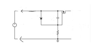
  • For hot plugging protection, I have seen something similar to the below circuit with a mosfet in

    systems that connect to an universal ac/dc supply  ie  "wall wart" supply.

    Other application I have seen adding TVS diode (eg SMDJ17) in automotive  or using a hot swap controller like a TPS24771 in servers .       

    The TPS24771 is suitable for hi rel systems that need to isolate the faults.   Zener diode may be a good for

    ESD but the probably does not have the energy capability needed from the hot plug.

    Can you send me your simulation file with test bench that has 10A into VIN?   

    The model is not that detailed to show a failure modes. 

    On the bench, if the VIN pin is sinking 10A, it will be after the pin experiences an overvoltage stress. 

  • Sent a mail, please check.