


Other Parts Discussed in Thread: UCC27624,
When using a SiC FET or sometimes an IGBT, you will find yourself needing a negative gate bias voltage. The negative bias voltage is often needed to pull the gate down enough to fully turn the switch off. Low side gate drivers (such as the UCC27614 and UCC27624) are typically referenced to the same ground as the controller and the power stage. In an example where bipolar drive (positive and negative gate drive voltage) is needed, the low side gate driver will be referenced to a negative bias; therefore the driver’s GND pin(s) will be connected to the negative bias.
In the example schematic (Figure 1), the negative bias is -5V (relative to GND), and the driver will be referenced to this so it can pull the gate of the switch to -5V.
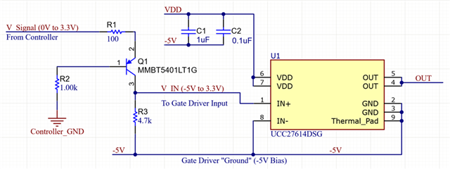
Figure 1: Example Bipolar Drive Schematic
The VDD voltage specification is an important consideration for bipolar drive applications, as the designer must include the negative bias as part of the VDD voltage range. If we use a VDD of 10V (relative to GND) for example, this would put a total of 15V across the driver, because we must add on the |-5V| from the negative bias. Using the UCC27614 from our example, it has a recommended maximum VDD voltage of 26V, so 15V is well within this range.
Now that we have our bias power, we must figure out how to reference our signal from the controller (that is referenced to GND) to the negative bias of -5V. This can be done with a simple level shift circuit based on a PNP BJT and a few resistors. The level shift circuit takes in the 0V to 3.3V PWM signal from the controller and shifts it to a PWM signal that swings from -5V to approximately 3.3V for the gate driver input pin. The schematic below shows a more focused view of the level shifter circuit.
|
ON condition |
When “V_Signal” is 3.3V, the PNP BJT is forward biased because the emitter is beyond a diode drop above the base. This allows the controller to then pull up the collector and therefore the input pin, bringing the input pin to approximately 8V relative to the negative voltage bias. This results in an ON signal for the gate driver. |
|
OFF condition |
When “V_Signal” is 0V, the PNP BJT is off and the R3 resistor pulls the input (and the collector) down to -5V, or 0V relative to the -5V negative bias. This results in an OFF signal for the gate driver. |
If your design has two switches that must be driven with a negative bias, then the same can be done with a dual channel low side gate driver such as TI’s new UCC27624. Everything will be the same, except you will have two level shift circuits; one for each channel input (as shown in Figure 2).
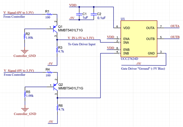
Figure 2: Dual Channel Solution
