This thread has been locked.

If you have a related question, please click the "Ask a related question" button in the top right corner. The newly created question will be automatically linked to this question.

TPS650864: Troubleshooting PMIC behavior used to power Xilinx ZU3.

Part Number: TPS650864
Other Parts Discussed in Thread: BOOSTXL-TPS650861, MSP430F5529

Hi TI team,

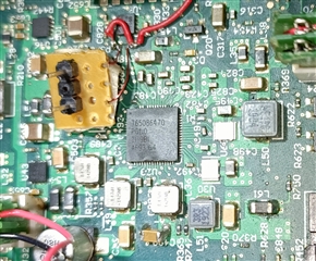
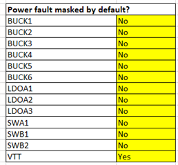
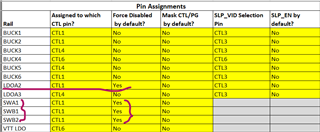
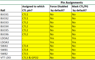
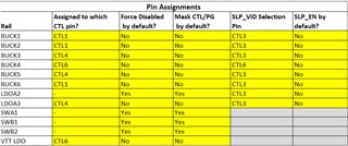
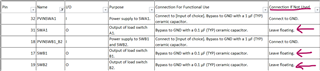
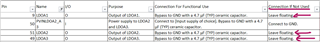
We recently replaced a PMIC after programming (burn) it with a custom OTP using TI BOOSTXL-TPS650861 along with MSP430F5529 LaunchPad Development Kit. We successfully burn the OTP which had configuration to disable LDAO1, LDOA2, SWA1,SWB1 and SWB2 as were are not using them in our design.

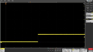
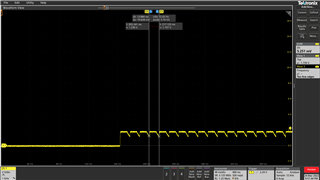
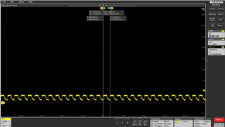
This new PMIC with custom OTP was replaced on to our board and when we powered ON, it worked as expected and then we did a power cycle (Off & then ON) and to our surprise we found that PMIC is in power fault state and then when we read the I2C registers , we came to know below facts,

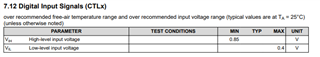
SHUTDNSRC: PMIC Shut-Down Event Register (offset = 05h) with data set to 05 means UVLO =1 and CRITTEMP=1. 

TEMPCRIT: Temperature Fault Status Register (offset = B4h) with data set to 1F means    DIE_CRIT, VTT_CRIT, TOP-RIGHT_CRIT, TOP-LEFT_CRIT, BOTTOMRIGHT_CRIT all are set to 1. 

Registers B0 to B3, B5 and B6 were all set to 00h means no issues.

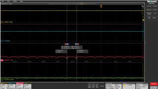
But we checked the Temperature externally using a thermocouple probe with multimeter, the temperature reading was within 34 degree C. 

So finally we turned PMIC OFF and waited for 5 to 10mins and then we turned ON and again to our surprise there were no power faults and all the expected rails were up and we even continued working on ZU3 by programming it, at this point we read the I2C registers and still it read same values as above. 

We repeated above steps for 7 times, and the results were same. (that is turn OFF the PMIC and wait for 5 to 10mins and then turn ON it works without any faults, but if you try to turn ON PMIC immediately or less then 5mins after OFF, then it goes into power fault state.)

Bottom line is if you give a time gap of 5 to 10mins between power cycles then PMIC works continuously for hours perfectly fine with no sign of power faults even though I2C registers reading shows above values.  

Can you please help me in debugging this issue.

Regards,

Sandeep P 

  • Hello Sandeep,

    We have assigned this ticket to the appropriate engineer who should be able to get back to you by Friday. Apologies for the delay.

    Regards,

    Alex

  • Hi Sandeep,

    Thank You for using E2E! I went through the information provided and here are my questions:

    • What is the orderable part number (and the top marking) for the PMIC that you are programming using BOOSTXL-TPS650861?
    • Could you please share you schematic along with the OTP generator that has the custom settings programmed on the PMIC? Let me know if you need to share these privately and I'll walk you through the steps to enable the private E2E message. 
    • Could you share a capture of the power-up sequence (after the power cycle) showing VSYS, V5ANA, LDO3P0 and LDO5P0? 

    Thanks,

    Brenda

  • Hi Brenda,

    Thanks for your reply. Please find the reply/information below that you have requested for,

    What is the orderable part number (and the top marking) for the PMIC that you are programming using BOOSTXL-TPS650861?

    Part number is : T65086470 PG1.0 TI 9BI AF93 G4

    Could you please share you schematic along with the OTP generator that has the custom settings programmed on the PMIC?

    Schematics:

    custom OTP Excel File attached.

    MID_PMIC_TPS65086100 OTP Generator V2p5.xlsx

    Could you share a capture of the power-up sequence (after the power cycle) showing VSYS, V5ANA, LDO3P0 and LDO5P0?

    Please find attached below,

     1) VSYS_12V0

    2) V5ANA

    3) LDO3P3

    4) LDO5P0

    Apart from above inputs, I do have a new observation about this issue. over the weekend the PMIC was running in power fault mode and when I returned to office on Monday and did a power cycle immediately (didn't wait for 5min to 6min) and to my surprise the PMIC was up and running without any power fault.  We repeated power cycle many times and it worked perfectly fine with no power fault. 

    Regards,

    Sandeep P

  • Hi Sandeep,

    Thanks  for providing an update and letting me know the PMIC is working as expected. I would recommend repeating the test, collecting the power-up waveforms on Buck1-6 (preferably all the waveforms in the same scope capture so you can evaluate the timing between rails) and making sure it follows the sequence that was programmed on the OTP.

     Please let me know if you see any issues. 

    Thanks,

    Brenda

  • Hello Brenda,

    Actually the power up sequence is normal and have not seen any difference in timing. The only issue noticed is after a continuous run if we do a power cycle then it shows fault and that is related to Critical temp register. But physically it not true as temperature is less than 34degC. Other than this there are no issues. 

    I have one more question to you, in our design we are using part number T65086401 PG1.0 TI 091 A7R0 G4, so can we actually burn our custom OTP into this part itself instead of using part T65086470 PG1.0 TI 9BI AF93 G4? 

    Regards,

    Sandeep P

  • Hi Sandeep,

    Do you also see the UVLO bit triggered in the SHUTDNSRC register? When you do a power cycle, are all supplies connected to the PMIC (including VCC_12V and VCC_5V_PMIC) cycled?

    Also, if you plan to use a pre-programmed OTP please review the OTP configuration in the datasheet as well as the pre-filled OTP generator to make sure all rails with power faults not masked by default have the proper external components. All the pre-programmed devices have rails that will not turn on until the previous rail's power good is asserted. Please let me know if you have any questions. 

    We do not recommend burning the second OTP bank on a pre-programmed device for production. This can also be done for prototype only if the TPS65086100 is not available. For production, if a custom NVM is needed, then TPS65086100 should be used. You can contact a TI approved distributor (like Arrow) for programming services.   

    Thanks,

    Brenda

  • Hi Brenda,

    Do you also see the UVLO bit triggered in the SHUTDNSRC register?

    Yes the UVLO bit is set to 1 and CRITTEMP bit is set to 1 , in SHUTDNSRC register. 

    When you do a power cycle, are all supplies connected to the PMIC (including VCC_12V and VCC_5V_PMIC) cycled?

    Yes all the power rails are turned OFF and then turned ON including VCC_12V & VCC_5V_PMIC. When we say power cycle we actually turning OFF the power source to the entire board and then turning ON.

    Also, if you plan to use a pre-programmed OTP please review the OTP configuration in the datasheet as well as the pre-filled OTP generator to make sure all rails with power faults not masked by default have the proper external components. All the pre-programmed devices have rails that will not turn on until the previous rail's power good is asserted. Please let me know if you have any questions. 

    Yes Brenda, We have verified them and ensured that all rails with power faults not masked by default (Except VTT). I had attached the OTP generator file for your review in my first reply also please find below snapshot of same. We are not seeing power fault in any of the rails when we read the registers but only when we probe in the scope we are able to see in buck 1 the fault pattern, Also at that time VSYS, LDO3P3, LDO5P0 and V5ANA all are normal expected levels. 


    We do not recommend burning the second OTP bank on a pre-programmed device for production.

    Any specific reason? Also the part that we have programmed with OTP is T65086470 not same as TPS65086100 as you mentioned above right? 

    Regards,

    Sandeep P

  • Hi Sandeep,

    Making register changes can be done in any of the TPS65086x devices but re-programming the default OTP configuration (burning new OTP settings) is not recommended. This could create multiple scenarios that have not been validated on our end.  


    We are not seeing power fault in any of the rails when we read the registers but only when we probe in the scope we are able to see in buck 1 the fault pattern

    Could you share a scope capture showing the "buck1 fault pattern"? Are all the unused rails in your design disabled/masked in the OTP? For  example, in your design, I see LDO1A1, LDOA2, SWA1, SWB1, SWB2 not used. These are the ones that should be disable and the corresponding power good masked. 


    Also the part that we have programmed with OTP is T65086470 not same as TPS65086100 as you mentioned above right?

    Yes, they are different. T65086470 comes pre-programmed to power Xilinx Artix7 and TPS65086100 is the user programmable version that must be chosen when none of the pre-programmed devices meet the power requirements. 

    Thanks,

    Brenda

  • Hi Brenda,

    Thanks for the explanation on not use OTP with T65086401 part.

    Could you share a scope capture showing the "buck1 fault pattern"?

    Buck-1 power fault

    Buck-6 power fault

    and Buck 2 was showing zero voltage.

    Are all the unused rails in your design disabled/masked in the OTP? For  example, in your design, I see LDO1A1, LDOA2, SWA1, SWB1, SWB2 not used.

    Yes, In the OTP file we have set these rails to be default disable and there outputs are all Zero. Below is the folder attached with waveform for all the rails, when PMIC is working normal.

      
    PMIC_All_Rails_output_waveforms.zip

    These are the ones that should be disable and the corresponding power good masked. 

    Since we have disabled the unused rails by default, we have not masked there PG and there is a note in that excel sheet which says so.

    Regards,

    Sandeep P

  • Hi Sandeep,

    I’m Brenda's teammate and I'll be helping you with this matter as well. Here are some next steps to take.  

    Yes, In the OTP file we have set these rails to be default disable and there outputs are all Zero.

    1) I noticed in your custom OTP document, you have LDOA1, LDOA2, SWA1, SWB1, and SWB2 set to "Force Disabled by default = Yes". The picture below is from the default OTP Generator setting for the TPS65086470. For disabled rails, it is recommended to disconnect them from the CTLx signals by choosing "-" in the "Assigned to which CTL pin" column. After that, both the "Force disabled by default" and the "Mask CTL/PG by default" sections should also be set to "Yes" for the disabled rails. The device may still work without this configuration but there may be some issues with power good detection if this format is changed.

    2) Could you please take a power up capture of VSYS, V5ANA, LDO3P3, and LDO5P0. Be sure to include all 4 signals in one capture so that it is easier to compare the ramp up timings.

    3) Please take a separate capture of the first 3 rails that should turn on in your sequence. Include all 3 rails in one capture, along with one of the signals from step 2 above if possible, so we can compare the ramp up timings again.

  • Hi James,

    1) I shall implement this on a fresh PMIC IC and solder it on the board. Meanwhile can please review and confirm if below snap reflect your review points?


    2) Please find the requested snapshot of all 4 waveforms (VSYS,V5ANA,LSO3P3 and LDO5P0).

    3) Please find the requested snapshot of all 4 waveforms (LDO3P3, Buck1,Buck2 and Buck6).

    Regards,

    Sandeep P

  • Hi Sandeep,

    Thank you for providing those captures. 

    1) Yes, that picture you shared of the "Pin Assignments" table is in line with my suggestion. Please note that the OTP can only be burned into the PMIC once. Bits that are burned as a "1" cannot be returned to "0" afterwards". Try this configuration and check the buck outputs again. If that doesn't work there are some other options.

    2)

    We are not seeing power fault in any of the rails when we read the registers but only when we probe in the scope we are able to see in buck 1 the fault pattern, Also at that time VSYS, LDO3P3, LDO5P0 and V5ANA all are normal expected levels. 

    Could you show a capture of VSYS, V5ANA, BUCK1, and BUCK2 in one image just so I can see the stable input voltage next to the buck outputs (or confirm that the above captures were taken with the bucks enabled). If the supply voltages are all stable, I'm led to believe that the issue may come from the output loads or the internal sequencing.

    3) I see that BUCK1, BUCK2, and BUCK3 all have more than one output connection. Could you disconnect all the loads and test the buck outputs? If the power fault behavior disappears then we can investigate the load conditions. What is the max load current you are expecting from BUCK1, 2, and 6?

    The periodic voltage drop in BUCK2 is propagating to BUCK1 and BUCK6 which makes sense based on your sequence programming. BUCK6 has the largest drop since it must wait for a "power good" signal from the both BUCK2 and BUCK1 before returning to the proper voltage level. I suspect that fixing BUCK2 should fix the other two regulators.

  • Hi James,

    1) Yes, that picture you shared of the "Pin Assignments" table is in line with my suggestion. Please note that the OTP can only be burned into the PMIC once. Bits that are burned as a "1" cannot be returned to "0" afterwards". Try this configuration and check the buck outputs again. If that doesn't work there are some other options.

    Yes we are aware that OTP can be burned only once. Hence I mentioned in my previous reply that I will  try this with a new  part T65086470. The software that we use to burn the OTP from TI has a feature that helps in verifying if the burn OTP is matching with what we had requested into registers. So just in case the "1" that cannot be return to "0" while we burn should flag us an error while we run this step. Till now we didn't see any such errors. And also after we burned the OTP we are physically checking the power up sequence on the BOOSTXL-TPS650861 board itself and didn't find any power faults or deviation from power up sequence.

    Could you show a capture of VSYS, V5ANA, BUCK1, and BUCK2 in one image just so I can see the stable input voltage next to the buck outputs (or confirm that the above captures were taken with the bucks enabled). If the supply voltages are all stable, I'm led to believe that the issue may come from the output loads or the internal sequencing.

    - Waveform capture for VSYS, V5ANA, BUCK1 and BUCK2 without any power fault.

    - Waveform capture for VSYS, V5ANA, BUCK1 and BUCK2 with power fault (when we turned OFF PMIC after a long run and then turned ON without any time gap).


    - same waveform as above but reduced time scale to capture power fault time interval.

    3) I see that BUCK1, BUCK2, and BUCK3 all have more than one output connection. Could you disconnect all the loads and test the buck outputs? If the power fault behavior disappears then we can investigate the load conditions. What is the max load current you are expecting from BUCK1, 2, and 6?

    The periodic voltage drop in BUCK2 is propagating to BUCK1 and BUCK6 which makes sense based on your sequence programming. BUCK6 has the largest drop since it must wait for a "power good" signal from the both BUCK2 and BUCK1 before returning to the proper voltage level. I suspect that fixing BUCK2 should fix the other two regulators.

    Yes we have more than one output connection. The loads on these bucks are, (Note: as of now we have not loaded the PMIC to the max values as mentioned below)

    i) Buck1- 1.85V has a load of 1.5 Amps

    ii) Buck2 - 0.85V has a load of 7.5 Amps

    iii) Buck6 - 1.2V has a load of 5 Amps

    Before I want to disconnect these each load and check for any issue, I would like to gentle remind you that when we allow a 5mins gap after a power cycle and turn ON the PMIC, all the output rails function normal without any power fault and we kept the board running for more than 5hrs or so and didn't find any issues. We even programmed the ZU3 FPGA and kept it running for long hours and found no issues. All these hours the load remained same. 

    So the question is do we really need to suspect the loads for this PMIC behavior? If so, then why after a time gap in power cycle makes everything work proper. 

    Thanks,

    Sandeep P

  • Hi Sandeep,

    Thank you for confirming the load and supply power conditions. It looks like your power supplies are stable and your loads are not drawing too much current. I am more convinced now that we are dealing with a power fault in the regulator sequence.

    • The PMIC checks for "power good" signals (PGOOD) about every 10ms. It looks like your voltage drops are occurring every ~13ms which would lead me to believe this power fault check is failing on one of the regulators and causing the rails to shutdown. When a power rail causes the fault, the PMIC only shuts down the regulators and reloads the OTP settings. After that it checks the CTL pins and tries to restart the regulators in sequence. Any of the regulators in your sequence could be sending the power fault signal. This behavior is described on page 56 of the datasheet (shown below).


      Could you provide a full register dump of all the OTP registers? Registers 0xB2 and 0xB3 (PWR_FAULT_STATUS1 and PWR_FAULT_STATUS2 respectively) could give us some insight into which rail is actually causing the power fault and resulting in all the rails to shutdown periodically.

      As I mentioned before, changing the OTP Generator table "Inputs to Enable" to the configuration I suggested might solve this issue by ensuring that the disabled rails are not being checked for a PGOOD signal. When you have implemented the new chip with the updated OTP settings, send me the new OTP Excel document for the record and let me know if the problem persists.

    • I noticed that LDO3P3 is used to pull CTL1 high with a pull-up resistor. We recommend to make sure that VSYS, V5ANA, LDO3P3, and LDO5P0 all reach a stable voltage before pulling CTL1 high. Note that the CTL1 signal is "undefined" from 0.4V to 0.85V according to the table in Section 7.12 of the datasheet (pictured below). If CTL1 is connected to LDO3P3, it may be turning on BUCK2 before the internal LDOs are at a stable voltage. BUCK2 is the most vulnerable to this issue since it only depends on CTL1 and does not look for a PGOOD signal from another regulator.


      This might explain why the PMIC functions normally for long periods of time as long as you wait 5mins after a power cycle and the start up process goes smoothly. That particular detail makes me think the issue occurs somewhere near the supply startup and CTL1. If a buck later in the sequence was the issue I don't see how waiting a long time before turning on the system would change the result. However I would still check the above mentioned registers just in case one of the later bucks is the culprit.
    • Below I will link two short "Frequently Asked Questions" posts that have a bit more detail on the functionality I described above. The images in the top linked post are similar to what you are seeing in your scope captures but I can't guarantee that the the issue you have is the same as what's described. The register dump and updated OTP Generator document should provide more insight.

      1) https://e2e.ti.com/support/power-management-group/power-management/f/power-management-forum/992402/faq-tps650864-regulator-is-shutting-down-or-measuring-x-lower-than-expected---what-is-the-cause

      2) https://e2e.ti.com/support/power-management-group/power-management/f/power-management-forum/971278/faq-tps650864-what-to-do-with-unused-voltage-regulators-rails?tisearch=e2e-sitesearch&keymatch=tps650864
  • Hi James,

    Thanks for the detailed reply. I am going through it.

    Since you are asking for the dump of all the OTP registers it looks like you had not got changes to see my first post regarding this issue (before Brenda replied me back). Can you please take a look at it ? (along with that following replies from me to Brenda). 

    I have attached the OTP dump for this issues below.

    PMIC_MID_Test_7.csv

    I am still working on getting the IC changed as our Lab Technician is little busy and i am waiting for my ticket number to be serviced. Once its done i shall give you a fresh dump of OTP from that IC and see if the issue is resolved.   

    Regards,

    Sandeep P

  • Hi Sandeep,

    Thanks for providing an update. James will go through the information and let you know if he has any questions. Once the PMIC (with the latest OTP config) is replaced on your PCB, please repeat the power-up test and let us know about the results.  

    Thanks,

    Brenda

  • Hello James and Brenda,

    Today we assembled the new PMIC which has a new OTP (with James suggested configuration implemented in it) burned in it. 

    The good news is this PMIC worked perfect without any power fault as soon as we powered it ON. We did power cycles and still it worked as out of datasheet. So our next plan is to replace the the Old PMIC which showed power fault with the New one and see if the performance repeats. Will keep you posted.

    Thank you guys for helping us out in resolving this issue. 

    But I would like to discuss with you about another topic and that is, why did we arrive at this situation of programming an OTP on a blank PMIC instead of using a production PMIC part directly assembled into our design. 

    Regards,

    Sandeep P

  • Hi Sandeep,

    I'm glad to hear that the PMIC is working as expected. Let us know if you see any further issues with the new device.

    In regards to your question:

    The TPS65086470 already has an OTP configuration burned into its first memory bank. This PMIC is designed to power a specific system (Xilinx Artix7). For PMIC versions such as this, non-volatile memory (NVM) registers cannot be changed and the PMIC will reset to its default settings after every power cycle. Only certain registers can be changed during PMIC operation and these volatile registers will not be saved upon a PMIC reset. The TPS65086470 does have a second memory slot that is blank and can be burned with a custom OTP configuration but we do not recommend using this method unless the TPS65086100 is unavailable. This other device is specifically for user programming and is described below.

    The TPS65086100 is the user programmable version of the same PMIC. This version has two blank OTP memory banks. The user can set up a custom OTP using the OTP Generator, and burn it into either of the memory banks. They can even burn two different OTP configurations using both banks. This PMIC version can be used to power a wide variety of systems as long as the custom OTP settings match the required specifications of the external system.

  • Hi James,

    Thanks for the clarification on the part TPS65086470,TPS65086100 and its usage.

    We actually don't want to use any of these blank IC's and custom OTP program to make it run in our design. Since our hardware design didn't follow the TI recommended configurations(checklist) while capturing schematics (unused pins like LDOA1, LDOA2 , SWA1, SWB1 and SWB2) we had to take this OTP path and make sure our present hardware design works for now.

    Please Note: We did refer the schematic checklist that was provide by TI and our schematics matches as per that, but in the checklist its not mentioned that you should have the rail disabled internally if you don't use as a resource like LDOA1 or LDOA2 and so on and just leaving it open or unconnected is not sufficient enough and that doesn't work or it also didn't mention that even if a rail is not used we have to provide a de-cap of 4.7uF and just leave it as is. So it was kind of a misled to us that, just following checklist was not enough and a review with TI engineer was important before we release the schematics for PCB design.

    So our main goal is to use production part TPS65086401 in our design, I shall modify our schematics to meet TI recommended schematics checklist along with the learnings from this OTP method and then send it for your review. Can you please share your email ID so that we can connect for this review and that shall close our main issue?

    Regards,

    Sandeep P

  • Hi Sandeep,

    I'm sorry to hear that the schematic checklist was misleading. In your case, the TPS65086401 OTP is pre-programmed to need certain rails (like LDOA1 and LDOA2) so even if the rails will not be used in your specific PCB design, the pin connections must still be populated with the correct external components. Once the external components are placed, the outputs of the rails can be ignored and not connected to an external system without issue. 

    One benefit of the user programmable TPS65086100 is that you can internally disable the unused rails with the OTP Generator, and once that is done you no longer need the external components since the PMIC will not look for a PGOOD signal from those rails. This means you can save space on your board.

    I'll send you a friend request so we can chat about the review if you need to send private information. If you have any other general questions about this device, please let us know here on the thread.