This thread has been locked.

If you have a related question, please click the "Ask a related question" button in the top right corner. The newly created question will be automatically linked to this question.

UCC28950: vmc

Part Number: UCC28950

Hi, 

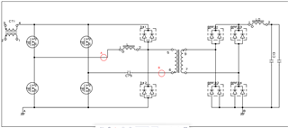
We are designing 5kW PSFB converter using UCC28950 as VMC.

For the secondary side, a full wave diode method was applied.
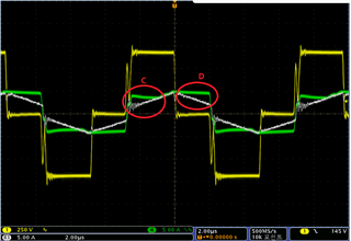
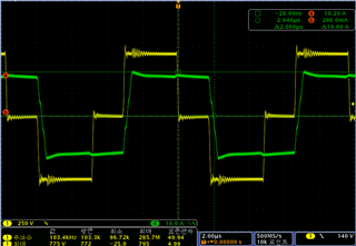
Fig 1

The waveform in Figure 1 are the primary side current and voltage waveforms measured under the 30% load condition.

When the DC blocking capacitor is applied at 2uF, the current in the red circle looks like a DC current.

In this state, the converter is damaged when it is operated for a long time.
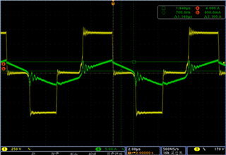
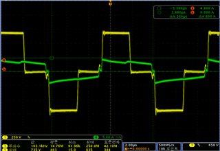
Fig 2.

The waveform in figure 2 is a waveform measured by adding a dc blocking capacitor and applying 5uF.

The dc current in the red circle in Fig.1 is not visible.

In this state, it is not be damaged even if it is operated for a long time.

What is the difference between the two current waveforms?

Can the current waveform tell us why the converter is broken? 

Or should I think there is a another reason?

And please advise on what criteria should be selected for the voltage withstand voltage of the DC blocking capacitor.

In terms of measurement, it is currently measured around 25Vp-p , 

but I have seen some data say that it has to withstand the input voltage.

Best Regards,

KW.

  • Hello,

    Please note your scope shots did not have a red circle on them.

    During the free wheeling period of figure 1 the primary is not showing the reflected inductor down slope across the transformer.  It looks like a flat spot and I believe that is what you are referring to as DC current. Did this waveform have a DC blocking capacitor? You mention it does and then you mentioned you added it in figure2.  If the DC blocking capacitor is not present.  In voltage mode control the transformer can saturate and that could cause the design to be damaged.

    The second waveform does not have the same flat spot and looks to be operating in critical conduction and current down slope during the free wheeling period looks to be correct.  The offset current in the first waveform during the free wheeling period causes a large current spike on the primary of the transformer when the converter comes out of the free wheeling period.  This may have something to do with the damage.

    Do any of these waveforms violate the maximum current ratings of the FETs and diodes used in this design?  The current spike on the first waveform could result in excessive voltages on the secondary if a shim inductor was not used with clamping 

    If you are using a shim inductor to achieve ZVS.  Please make sure you have clamping diodes between the shim inductor and the input of the transformer.  This will help prevent damage when coming out of the free reeling period.  The following link will bring you to an application note that describes how to design with a UCC28950 in a phase shifted full bridge.  The clamping diodes are shown in figure 1, the diodes are DB and DC.

    https://www.ti.com/lit/an/slua560d/slua560d.pdf

    Regards,

  • Hi, Mike,

    Thanks for your reply.

    The waveform in Figure 1 was also measured with the dc blocking capacitor. The difference between fig1 and fig 2 is the difference in the amount of dc blocking cap. Fig 1 is 2uF and fig 2 is 5uF.

    Is the DC current shown in Fig 1. due to the lack of a dc blocking capacitor?

    If there is DC current, can you think of it as transformer saturation?

    Is there a withstand voltage of the dc blocking cap?

    When measuring the voltage across the dc blocking cap with an oscilloscope, it is unlikely that a large withstand voltage will be required.

    And the product under test currently uses a shim inductor and does not have a clamp diode. There seems to be insufficient information about the capacity of clamp diode. There is a saying that formula in datasheets are the worst case.

    Is there any way to determine the current capacity of the clamp diode?

    Best Regards.

    KW

  • Hello,

    Transformer saturation generally present it self like a parabolic ramp getting very steep.   It generally does not show up as a flat spot.  The flat spot during the freewheeling period should be a representation of  the output current reflected across the transformer.  This is where you are seeing the flat spot on figure 1.  During this time interval either FETs A and C or B and D are shorting the primary.  This does not look like transformer saturation to me.

    The flat spot has to being cased by the secondary the primary of the transformer is shorted.  The capacitor you added is some how affecting the secondary current.  Not sure how that current is being developed or changed.  You might want to study the voltage across the shim inductor and the input and output of the transformer to see if you can see a strange behavior.  If you don't there is something on the secondary that is causing that behaivor.

    I think your design is being damaged because your design is not using the clamp diodes.  When you come out of the freewheeling period the output current is reflected across the transformer.  At this time there is no current in the shim inductor.  The shim inductor will not accept the current right away because inductors do not except immediate changes in current.   This will cause excessive voltage across the primary of the transformer that is reflected to the secondary and can cause damage.  I believe if you add the clamp diodes this will remove your issue.

    Regards,

  • Hi, 

    I am testing by connecting a clamp diode as recommended.

    It is connected as shown in the circuit diagram below.

    The waveform below is a measurement of the current at points A (Green) and B (White) in the diagram.

    Point D of the waveform will be understand.

    But is point C correct?

    Even if I try the simulation, point C does not come out.

    I wonder if it is working properly.

    The current waveform is measured at about 20 % of the load.

    As the load is gradually increased, C and D approach almost equally.

    Regards.

  • Hello,

    The white waveform is correct and that is what the transformer current should look like.

    The flat spots on the input of your shim inductor current indicate there is a constant voltage across it. Both during the energizing period and freewheeling period.  

    di =V*dt/Lshim

    Your shim inductor might be too large forming a voltage divider with the primary magnetizing inductance.  It's current is larger the transformer magnetizing current and reflected output current.  I think if you shrink the shim inductance you may remove this behaivor.

    Regards,

  • Hello,

    Thanks for your reply.

    The shim inductance was reduced, and the following waveform was obtained.

    This is the result of reducing the existing 8uH to 2uH.

    The following is the result of lowering the output inductance.

    As it was closer to the desired waveform, the load was increased in this state.

    The following the waveform measured in the final 5kW state.

    In this state, Qc and Qd Mosfet performed thermal runaway.

    Is the waveform affecting Qc and Qd?

    Or can you think that the waveform itself is okay?

    Regards.

  • Hello,

    You shim inductor is supposed to help with ZVS.  You might want to see what performance you get without it.  Some designer choose not to use it.

    The transformer primary currents looked o.k.  it is just the shim inductor current that is strange.  Nothing looks to be saturating

    Regards,

  • Hello,

    You still want to look at the transformer current and CS as well.

    Thermal runaway in FETs C and D seems strange.  This means during free wheeling there is excessive current going through these FETs.

    I would double check the FETs to make sure they are turning on and off correctly I would study the Vgs voltages compared to the Vds voltages. 

    Regards,

  • Hello, 

    I still have thermal issues with FETs C and D (lagging leg).

    The temperature difference with the leading leg is about 20 degrees.

    Vgs and Vds are shown below. (Yellow : Vds, Blue : Vgs of QD)

    ZVS seems to be working fine, but the heat is not decreasing.

    Reducing the deadtime still does not solve the problem.

    Even if the positions of the leading leg and the lagging leg are changed on the same PCB, the temperature of the lagging leg is still high, 

    so it seems that it is not a PCB problem.

    Are there any strange parts in the waveform or other test methods worth trying?

    Regards.

  • Hello,

    Why does your wave form have what appears to be a small resonant ring just as the drain voltage is going from its highest point to lowest point.

    The  waveform should look similar to what is below.

    For some reason I think you might be hard switching on the CD leg.  However, the CD leg generally achieves ZVS first and I am not seeing the miller plateau.

    I think you need to study the current through the CD and AB FETs to see what the difference is.  The current should be roughly the same and if it is not then you have to figure out where the excess current is coming from that is making FETs C and D hot.

    Regards,