This thread has been locked.

If you have a related question, please click the "Ask a related question" button in the top right corner. The newly created question will be automatically linked to this question.

BQ25300: Charging stops and STAT led keeps blinking after a period of normal operation

Part Number: BQ25300

Hi everyone,

I have been struggling with the design of a power management module that has among other smps regulators the BQ25300.

I baked the components at 60 deg celsius for 12 hrs just to be sure and used a stencil to apply the solder paste to the pcb an eventually used a hot air gun.

This chip has been the center of my torture after trying the 3rd prototype. It makes me wonder since i have got a xmega16 VQFN, a boost converter and a buck converter and all of them have been working without the slightest instability.

So, after assembling the 3rd prototype, everything worked fine for a few days and then the STAT led started blinking w/o obvious reason. No matter what i did the STAT led would always blink. I noticed that some times the STAT led would stop blinking and the charge current would be the expected value (charging would start). After removing the VIN and retrying, the STAT led would again keep blinking. I tried LiPo batteries at various charge levels with their voltage anywhere between 3.0 and 4.2V. The STAT led would keep blinking.

I checked the conditions that would normally lead to a fault but could not find anything useful.

My VIN has always been 5.0V. The forward voltage drop of the input diode is not a problem since it reaches 400mV @ 2A @ 55 deg which means that a fully charged bat (4.2V) would still be less than the effective VBUS which is 5.0V-0.4V=4.6V

VVBUS > VVBUS_OVP
Thermistor cold/hot fault on TS pin
VBAT > VBAT_OVP
Safety timer fault
ICHG pin is open or short to GND
Die temperature is above TSHUT

This is the schematic designed in KiCAD:

For testing purposes i removed the R3 and connected another R 10-20K from VBUS to EN pin so that the chip is always enabled. POL has been tied to GND, so setting EN to a high logic enables the charging.

The max temperature i detected with a thermal camera was 70 deg celsius for a short period across which the current was almost 2A as set by R5.

The NTC used was the 103AT.

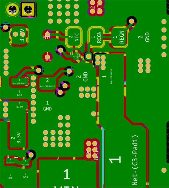
Here are some snapshots of the 6-layer pcb for your reference. I don't expect PCB design analysis off course:

TOP LAYER

TOP LAYER

INNER LAYER 1

INNER LAYER 2

INNER LAYER 3

INNER LAYER 4

BOTTOM LAYER

I am thinking that the culprit could be any of the following:

  • Some decoupling mlcc with the wrong ESR (more or less than required)
  • PCB design bad practices E.g: decoupling caps away from a pin etc
  • Pop-corning effect having destroyed the die during reflow (i used 300 deg celcius)
  • Inherent instability issues from the chip itself (unlikely)
  • Some component wrong value

Can anyone please help because i am on deadline here at work and i do not want to use a crappy way of charging the battery since i need to have this ready in less than 10 days.

Regards to all.

Manos Tsachalidis

  • Hi Manos,

        What is the frequency of STAT oscillation? Can you take a waveform of VBAT, VSW and VSTAT?

  • Unfortunately i have unsoldered the IC at the moment. However, i am sure the STAT led was blinking at 1Hz as per the datasheet. I will solder one new chip to the pcb and get back to you.

    Apologies.

    Manos

  • Sounds good. Once IC is re-soldered, it would be a good idea to log measured DC voltages of the pins as well and report here.

  • One thing i would like to ask you, if you don't mind, concerns the fact that the ICs i have in hand have been opened from their bug (mouser's bug) and have been subjected to humidity which here in Cyprus is >80%. I am afraid that i have to bake the IC before soldering. I have had serious issues with components not operating normally due to pop-corning effect which was solved after baking the components! Any advise on that? Should i just reflow the IC with hot air? Should i take it slowly to up 100 deg celsius for a minute and then keep going higher?

    Any advise would be highly appreciated.

    Regards

    Manos

  • Hi Manos,

       Baking the components is recommended for high humidity out of package, and soldering pretty quickly after baking is recommended. I am not exactly sure what the MSL of this QFN with 0.5mm pitch would be so I would have to check and get back to you. I would assume at 125C for a couple of hours should do the trick.

  • Ok thanks i can do 125 deg celsius for 2 hours! I will get back to you when i reflow the component.

    Thanks

    Manos

  • Hi Kedar,

    Good news. The IC is working at the moment. I get an accurate 2.0A charging current as per R5 (20K) and a max temperature of 65 deg celsius. I am a bit surprised i get these temperatures given the 6-layer pcb. This was intentionally done with most layers being connected to the IC's thermal pad! Charging current started ramping down over 4.1V and keeps getting lower. I have a crappy logger in place sent by the uC to my linux PC. It is now at 4.17V and current at around 900mA.

    Seems stable for now.

    I did a 2.5 hrs baking at 125 deg celsius. After re-flowing which was really tricky (if not done well the first time) i got a non-working state with the STAT led being constantly lit and a dummy current at VIN of 37mA. After re-soldering with the soldering iron, cleaning thoroughly with 90%+ alcohol and checking with a microscope it worked.

    However, i am not feeling very confident. It may stop working on the 3rd or 5th day and i have no way of telling when. Let's hope this was just a problematic soldering issue.

    I am really grateful for your time.

    My best regards

    Manos

  • Hi Kedar,

    Bad news. And we are back to the beginning. This morning, i connected 5.0V to the VIN and the STAT led started blinking. Yesterday, it was all working fine. I am not sure anymore... Ok there is something weird. I started touching my finger on the PCB exactly where the PMID MLCC was and the STAT led went constantly on, the charging current was normal and it stayed there. It would then stop/start randomly if i keep touching the PMID pin. Putting force on it with an insulated object would not change the charging status. I thought that the PMID could be faulty, so i replaced it. That cap is supposed to be 10uF. I chose 10uF/25V. The problem persists. If i touch the PMID charging will commence at randomly. But later i found out that touching on the system GND would also have the same effect. Really weird... Any ideas?

    Regards

    Manos

  • Would it help if i increased the cap at the PMID pin? Not sure what to think anymore... Do you want me to get the waveforms you asked for at the first place?

  • One thing worth mentioning is that the VBUS decoupling cap is at the bottom layer. There was simply no room on the top layer. It is directly under the VBUS pin though. I put plenty of VIAS there...

  • It is possible you have an issue with your ground routing? PMID capacitor should be placed with highest priority close to PMID pin of charger IC. You can also try adding a decoupling cap onto PMID of around 10nF and 100nF to see if this helps shunt out any high frequency noise. From a decoupling cap perspective, adding a decoupling cap on PMID will do much more than adding one on VBUS.

  • Thanks for your message.

    I think this has got something to do with decoupling caps too.

    *At this time, the IC works fines. Nothing changed since i soldered the last IC above. Suddenly it just started working. I will add a 100nF in parallel with the C7 though. Seems like a good idea!

    Here is the top layer. C7 is the PMID cap.

    This is the bottom layer

    Maybe this can help you have a better idea of the pcb itself.

    Regards

    Manos

  • Hi Manos,

       C7 looks close from a layout standpoint so this is good. From a layout priority, if there is a enw board rev planned, we would want to prioritize the decoupling cap placement close to the IC pin of PMID, and then the main PMID cap. For now, you can try soldering the decoupling cap on top of the main PMID cap and see if you don't see the issue anymore.

  • Hi Kedar,

    You got me confused there!

    You 're talking about two caps both connected to the PMID pin...

    Do you mean that i have to prioritize placing the VBUS decoupling cap C3 on the top layer instead of the bottom?

    The PMID cap is close enough i think but could be placed a bit closer i suppose. I remember you talking about placing a 100nF cap in parallel with the existing C7 10uF cap which could help filtering out high frequency content and eventually make the IC's operation more stable.

    All MLCCs are X7R and the highest voltage rating i could find to minimize capacitance degradation due to biasing. Currently C7 is a X7R 10uF/25V (regardless of the 16V rating seen in the schematic.

    Currently as mentioned in a previous post, operation seems stable. So placing a 100nF in parallel with the C7 PMID cap is not gonna change anything but i will do it anyway to hopefully minimize the chances for the IC to suddenly stop working.

    Please confirm.

    Regards

  • Hi,

      Yes decoupling caps would theoretically be a 2nd cap, like an 0402 package with 0.1uF of 0.01uF value. You would place the decoupling cap closest to PMID pin, and the actual PMID cap right after. From a decoupling cap perspective, you would want the decoupling cap as close as possible on the top layer, but the VBUS decoupling cap is not as important as the PMID decoupling cap. PMID is the true input to the switching converter.

  • Thanks Kedar,

    I will do that.

    Although i do not have a 100% proof that the caps at PMID pin is the culprit, i will set this thread to resolved since i think this is most probably the issue i am facing here.

    Thanks again.

    Regards

    Manos