This thread has been locked.

If you have a related question, please click the "Ask a related question" button in the top right corner. The newly created question will be automatically linked to this question.

UCC256303: LLC UCC256303 noise on output

Part Number: UCC256303
Other Parts Discussed in Thread: UCC24612

Hello. I am trying to make an LLC converter for 300W using the UCC256303, with synchronous rectification using two UCC24612 on the secondary side.

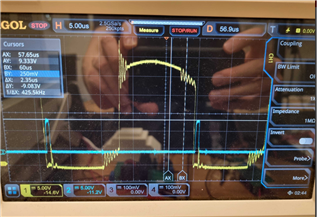
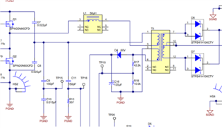
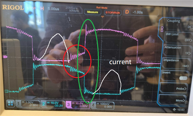
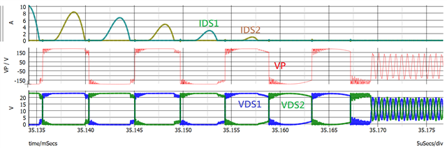
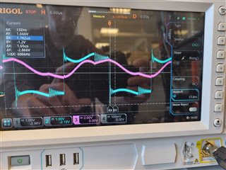
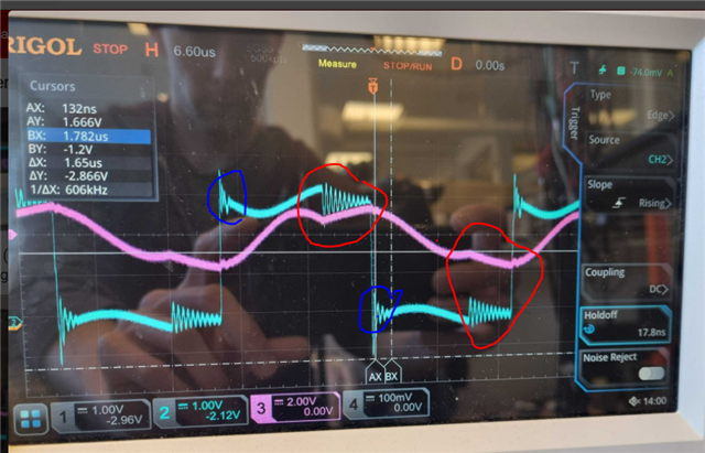
Below you can see the measured voltage on the drain on one of the rectifying mosfets (yellow) and the gate signal from the UCC24612 (blue) on the secondary side. The other mosfet & UCC24612 pair is behaving in the same way. The noise causes problems for the synchronous rectification, as the UCC24612 triggers prematurely. My circuit is looking very similar to the eval board of the UCC256303. I attached a figure of the resonant part of the schematic. 

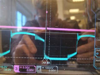
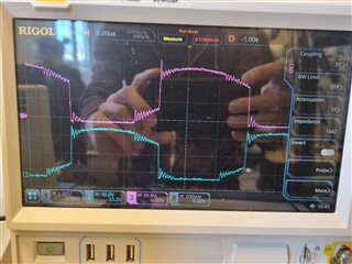
What could be the cause of this noise? I measured on the resonant capacitors (between C7, C8) and I'm getting a nice sinusoidal wave without noise. Then I measured between the external inductance and the transformer (L1, T1) and there I'm getting similar noise as the picture below. 


  • Hi, Niclas:

    Thanks for reaching us. Let's figure out where the noise from. I may need your help to check the VDS of another MOSFET. 

    i.e, if the waveform you shared is the VDS and Vgs of Q1, I would need you help to check VDS(Q1), Vgs(Q1) and VDS(Q2).  Since there is a voltage ringing when VDS goes high. The noise might from VDS ringing from another SR MOSFET. 

    btw, would you mind to share your schematic, or the part of UCC24612? 

    Regards, 

    Wesley

  • Here is Vgs and VS of the other pair, and also VDS of both rectifying mosfets. The noise has a frequency of 2.7MHz. My schematic is a mess. You can consider it the same as the picture in the first post, except with the diodes on the secondary replaced by mosfets.

  • Hi, Niclas:

    May I know if this phenomenon shows full load range or just happens at light load? The VDS ringing may be caused by not enough resonant current to sustain the voltage of Vp (pin3-pin4 of transformer).

    I uses the UCC256404's simulation and the results similar to yours. So it needs you check it again in your circuit.

    Would you please try to increase output load and see if this ringing gets smaller? If so, to increase Lp/Lr ratio would be helpful to improve this ringing. 

    Regards, 

    Wesley

  • I tried to increase the load. The waveforms changed shape a bit but I wouldn't say the ringing became smaller. The left image is with very low load, 10W. The right is with 100W. 


    I measured Isense on the primary (R13 in the schematic above) and the voltage at the node between L1 and T1. Purple is the current and blue is the voltage. Does this tell you anything?


  • Hi, Niclas:

    I think your waveform aligned with my previous post. The there is no current delivery to 2nd side in red circle. So transformer is demagnetized. VDS or Vp starts freewheeling and it caused voltage ringing.


    Based on the waveform of both 10W and 100W, the portion of demagnetized zone does not change a lot. That's the reason that the ringing is not smaller as load increased. The spike in blue circle comes from the di/dt of transformer inductance. It may be lower when you increase Lp I think. 

    Back to UCC24612, since there is a VDS spike in blue circle, and it would trigger VG on/off unexpectedly. You can add a resistor (around 1kohm~10kohm) between IC VD pin to MOSFET drain to eliminate the noise to IC VD pin. To optimize resonant tank design is also a way to reduce the ringing. 

    Regards, 

    Wesley

  • A better optimzed resonant tank helped. But I was also using a too low input voltage. When I increased from 320V to 390V it improved. I was switching at below resonance.